Secondary electron measurement device

A technology of secondary electrons and measuring devices, applied in measuring devices, material analysis using wave/particle radiation, instruments, etc., can solve the difficulty of receiving reverse electrons, the difficulty of measuring the degree of neutralization of implanted ions, and the systematic error of measurement and other issues, to achieve the effect of small bombardment damage, realize total current measurement, and avoid surface damage

Active Publication Date: 2017-05-31
CHINA INSTITUTE OF ATOMIC ENERGY
View PDF6 Cites 6 Cited by
  • Summary
  • Abstract
  • Description
  • Claims
  • Application Information

AI Technical Summary

Problems solved by technology

There are two difficulties in the ion implantation method. One is that the implanted ions are easy to cause surface damage, and the surface damage will affect the emission performance of secondary electrons. The other is that it is difficult to measure the neutralization degree of implanted ions, and the equipment is also complicated and expensive.
The use of thin samples will affect the emission performance of secondary electrons
[0007] The second problem is that when the primary electrons gene...

Method used


Image

  • Secondary electron measurement device
  • Secondary electron measurement device

Examples


Embodiment 1

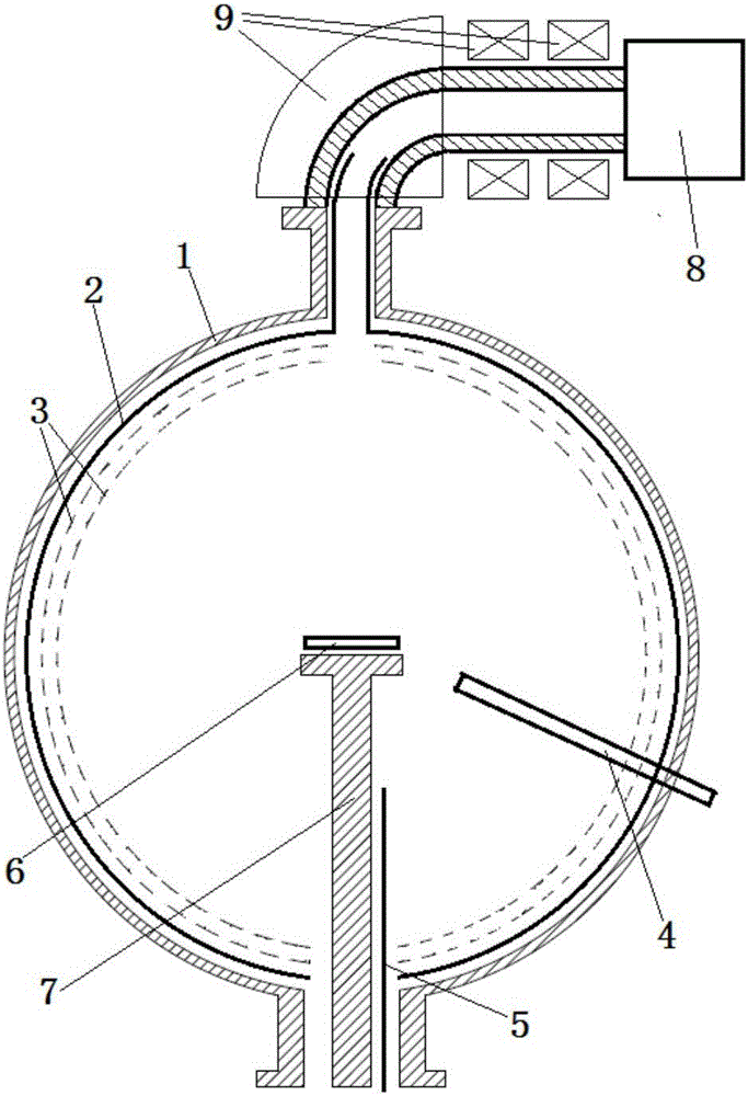
[0027] Such as figure 1 The secondary electron measurement device shown is composed of a vacuum chamber 1, a receiving electrode 2, a grid 3, a plasma torch 4, a plasma excitation electrode 5, a sample to be tested 6, a sample carrier 7, an electron gun 8, and an electron deflection transmission system 9 And other systems such as vacuum, power supply, and measurement.

[0028] The sample carrying bracket 7 is set in the vacuum chamber 1, the sample 6 to be tested is set on the sample carrying bracket 7, and the primary electrons are emitted by the electron gun 8 into the vacuum chamber 1 and bombard the sample 6 to be tested, which can be loaded with high-pressure plasma The excitation electrode 5 and the plasma torch 4 can be set separately or at the same time. After completing the secondary electron measurement of one or several electron pulses of the sample 6 to be tested, close the vacuum pump valve of the electron gun and the vacuum chamber, and pass the The plasma gener...

Embodiment 2

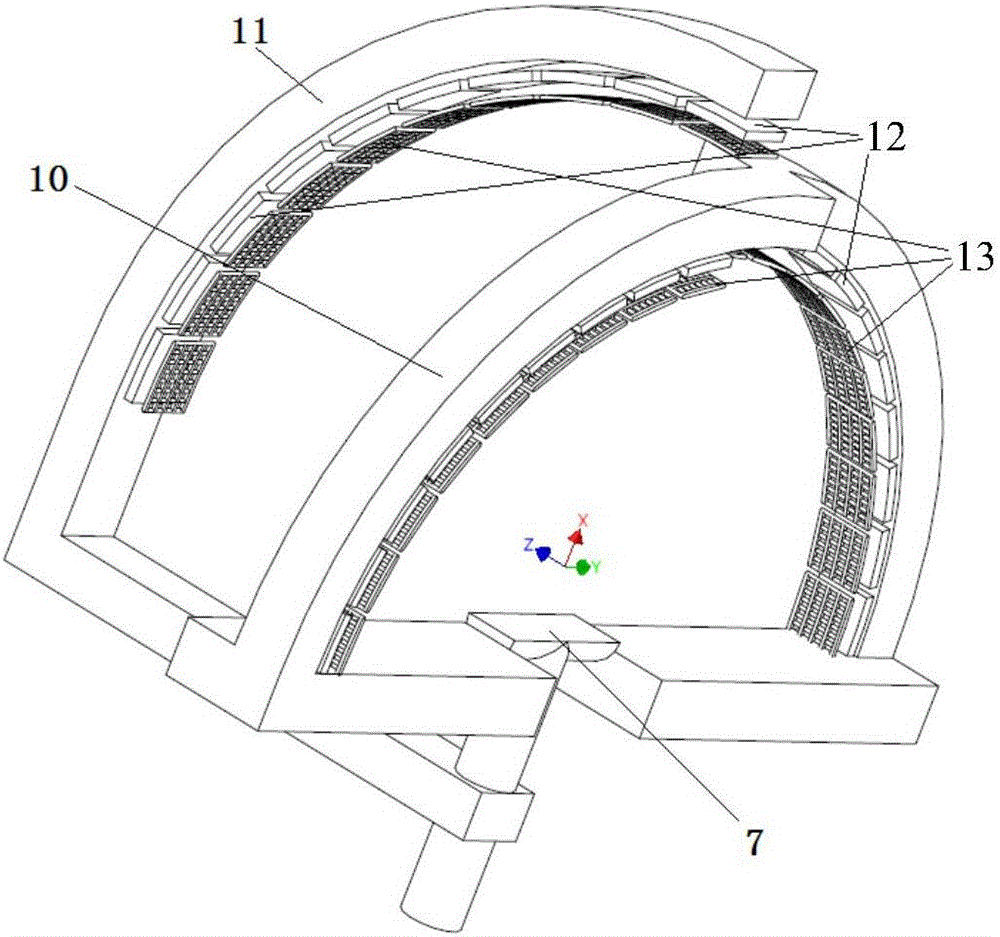
[0036] figure 2 Shown is the secondary electron current angular distribution measurement bracket diagram. When measuring the angular distribution of the secondary electron current, the figure 1 The receiving electrode 2, the grid 3 and the electron deflection transmission system 9 in the measuring device are removed, the electron gun can directly shoot into the sample to be tested, and the sample carrying bracket 7 is changed to figure 2 Structure.

[0037] figure 2 Among them, the Y-axis turret 10 can independently rotate along the Y-axis parallel to the surface of the sample to be measured relative to the sample-carrying bracket 7; X-axis rotation; the sample carrying bracket 7 , the Y-axis turntable 10 and the X-axis turntable 11 can rotate together along the Z-axis parallel to the surface of the sample to be measured and perpendicular to the Y-axis. On the inside of the Y-axis turret 10 and the X-axis turret 11 relative to the sample, a mutually insulated secondary ...


PUM


Abstract

The invention belongs to an electron measurement technology and particularly relates to a secondary electron measurement device. According to the device, a plasma generation device is arranged in a vacuum cavity, charges accumulated on the surface of an insulated sample during secondary electron measurement are neutralized by plasma, and total current measurement and angle distribution measurement of secondary electrons can be realized; secondary electrons of a reverse-shooting electronic gun can be collected. The problem of surface damage of the insulated sample with a positive ion implantation and neutralization method in the prior art is solved.

Description

technical field [0001] The invention belongs to electronic measurement technology, in particular to a secondary electronic measurement device. Background technique [0002] Secondary electrons refer to electrons with certain kinetic energy that bombard the surface of some materials and emit electrons from the surface of the material. The energy of secondary electrons is very low, generally no more than 50eV, and the conditions for its generation are generally vacuum. [0003] For different application environments, the impact of secondary electrons has its own advantages and disadvantages. In high-power waveguides, the emission of secondary electrons can easily lead to radio frequency ignition, making the microwave transmission system unstable. In the radio frequency resonant cavity, especially in the superconducting resonant cavity, the secondary electrons are easy to cause avalanche effect and spark, which will also make the resonant cavity unable to work stably. Theref...

Claims


Application Information

Patent Timeline
IPC IPC(8): G01N23/225
CPCG01N23/225
Inventor 李金海
Owner CHINA INSTITUTE OF ATOMIC ENERGY
Why Eureka
Try Eureka