Piezoresistor and manufacturing process thereof

A piezoresistor and electrode technology, which is applied in the manufacture of resistors, piezoresistors, resistors, etc., can solve the problems of piezoresistor flow capacity drop, electrode offset, side flashing, etc., to reduce typesetting The effect of inspection, edge density improvement, and long dwell time

Active Publication Date: 2017-05-31
KUSN WANFENG ELECTRONICS
View PDF7 Cites 11 Cited by
  • Summary
  • Abstract
  • Description
  • Claims
  • Application Information

AI Technical Summary

Problems solved by technology

[0005] The eccentricity of the electrodes not only leads to a decrease in the flow capacity of the piezoresistor, but also tends to cause side flashes. In severe cases, the electrodes even shift to the side of the ceramic substrate and are directly connected

Method used


Image

  • Piezoresistor and manufacturing process thereof
  • Piezoresistor and manufacturing process thereof
  • Piezoresistor and manufacturing process thereof

Examples


Embodiment 1

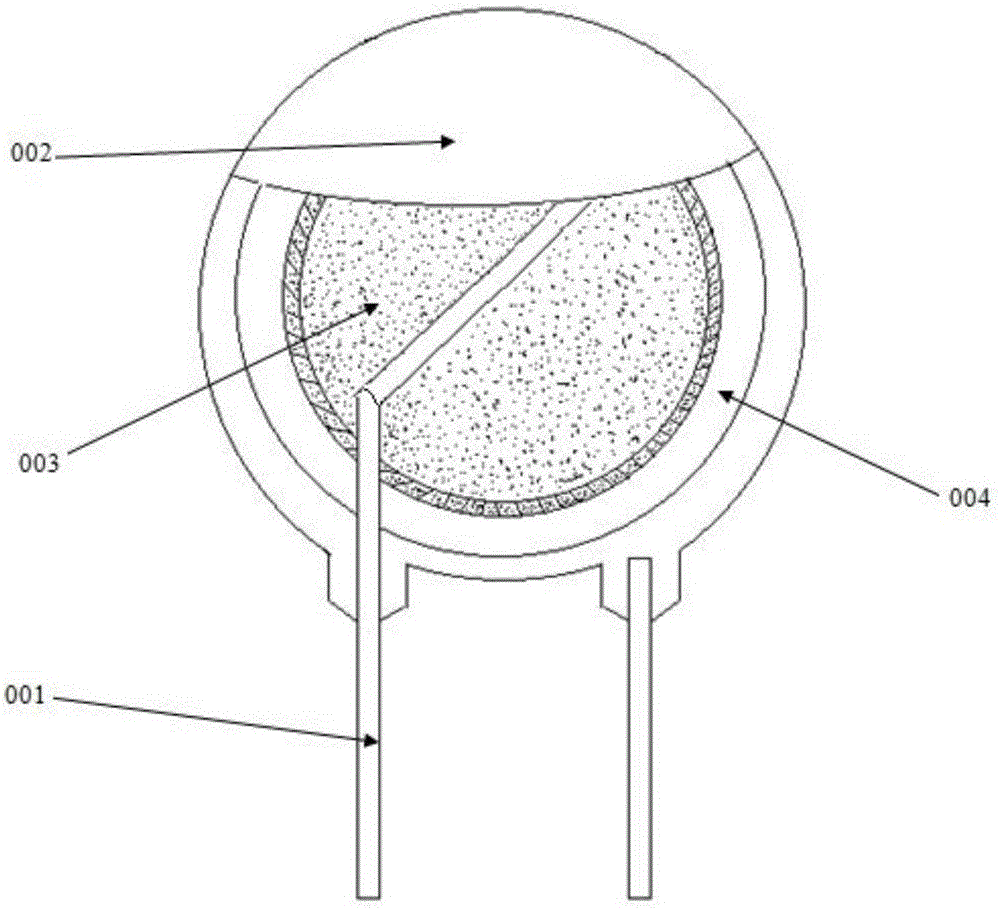
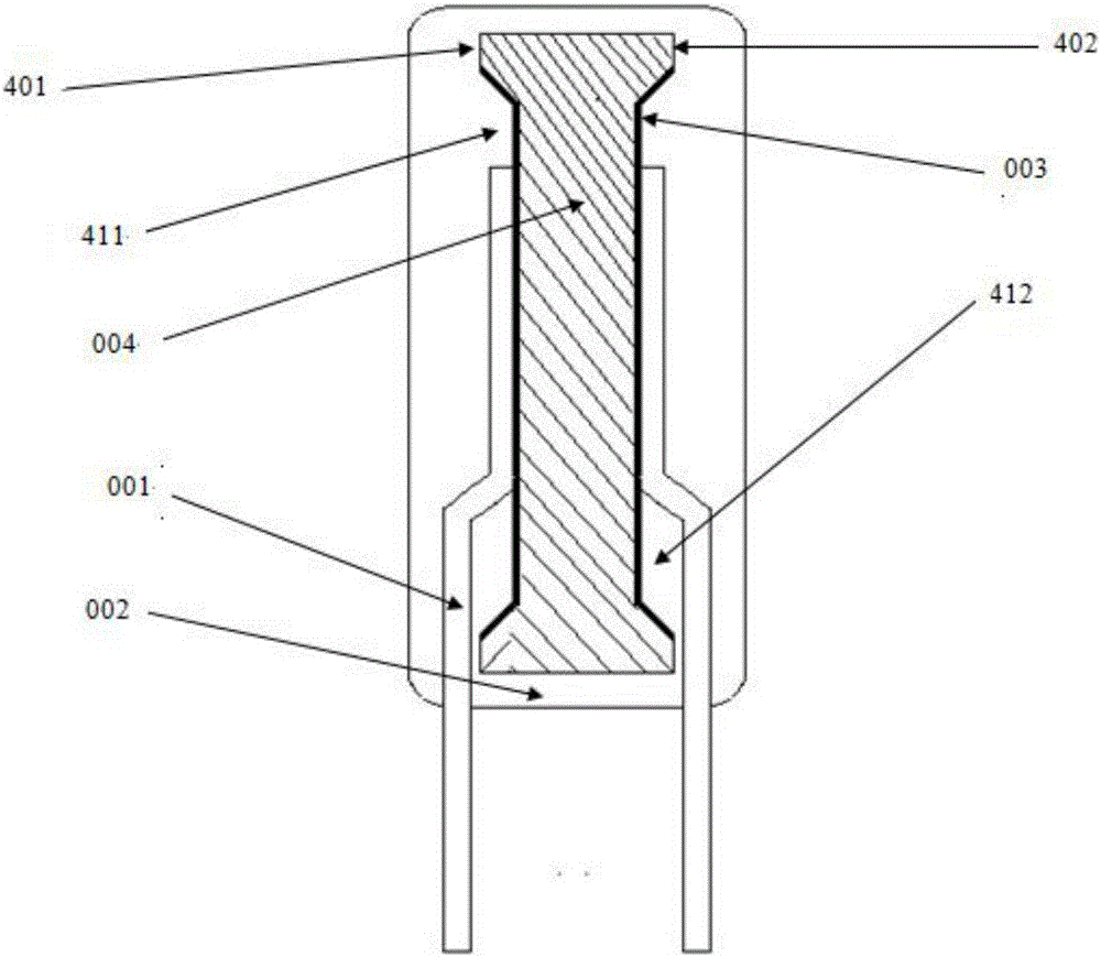
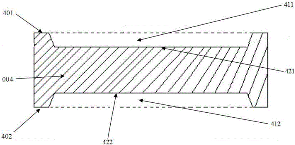
[0029] Embodiment 1, see attached figure 1 , 2 , 3, the present invention relates to a varistor, which includes a lead end 001, an insulating layer 002, an electrode layer 003 and a ceramic substrate 004, the ceramic dielectric substrate 004 is circular, and the ceramic substrate 004 The upper and lower bottom surfaces 401, 402 each have a prefabricated concave electrode area 411, 412, the bottom surface 421 of the prefabricated concave electrode area 411 is parallel to the bottom surface 401 of the ceramic substrate 004 where it is located, and the bottom surface 422 of the prefabricated concave electrode area 412 is parallel to the ceramic substrate 412 where it is located. The bottom surface 402 of the substrate 004, the bottom surface 421 of the prefabricated concave electrode region 411, and the bottom surface 422 of the prefabricated concave electrode region 412 are all circular, and the depths of the prefabricated concave electrode region 411 and the prefabricated conca...


PUM

PropertyMeasurementUnit
depthaaaaaaaaaa

Abstract

The invention relates to a piezoresistor and a manufacturing process thereof. The piezoresistor is composed of a ceramic substrate, a leading-out end, an electrode layer and an insulating layer, wherein a concave area, namely, an electrode positioning area, is prefabricated on the ceramic substrate; the leading-out end is arranged on an electrode; the insulating layer is used for locally or wholly packaging the ceramic substrate, the electrode layer and the leading-out end; in the manner of sputtering or spraying electrode, an electrode hole of a mask plate is positioned and coated on a concave opening; a small electrode hole and a big concave opening form a bottle-shaped structure; the electrode is drifted and deposited into the concave opening so as to form the electrode and realize the concave opening being accurately filled with the electrode; the electrode eccentricity caused by the difference in diameter of the ceramic substrate in a batch sputtering process can be avoided; the thickness of the ceramic substrate at an edge of the concave opening is greater than the thickness of the interior; the reducing of the risk in edge arc crossing is benefited; the edge effect is weakened; the flowing property is greatly promoted; the preparation process of the piezoresistor comprises the following steps: manufacturing the ceramic substrate, performing electric polarization, connecting the leading-out end, coating the insulating layer, printing and testing.

Description

technical field [0001] The invention relates to the field of piezoresistor manufacturing, in particular to a piezoresistor and a manufacturing process for synchronously prefabricating a concave electrode area during a molding process. Background technique [0002] Due to its good voltage limiting characteristics, varistors are widely used from weak current systems to strong current systems, from electrostatic protection, SPD valves to lightning arresters, from line surge protection to motor demagnetization energy absorption. When the suppression voltage is turned on, it is close to a short circuit, so the overlapping size of the two electrodes is similar to the diameter of the wire, which directly determines the flow capacity of the product. [0003] Considering that the thickness of the electrode affects the current diffusion and current carrying capacity, the surface metallization methods commonly used in electronic ceramics, electroplating and evaporation are not suitable...

Claims


Application Information

Patent Timeline
Patent Type & Authority Applications(China)
IPC IPC(8): H01C7/10H01C17/00
CPCH01C7/10H01C17/00
Inventor 李伟力李国正阙华昌周慧方弋褚平顺
Owner KUSN WANFENG ELECTRONICS
Why Eureka
Try Eureka