STT-MRAM storage unit

A technology of memory cells and seed layers, applied in electrical components, electrical solid-state devices, circuits, etc., can solve problems such as slowness, technical difficulties, and difficulty in adjusting the anisotropy constant K, etc.

Active Publication Date: 2017-05-31
XI AN JIAOTONG UNIV
View PDF6 Cites 10 Cited by
  • Summary
  • Abstract
  • Description
  • Claims
  • Application Information

AI Technical Summary

Problems solved by technology

On the one hand, the anisotropy constant K is usually determined by the interface technology and material type of the magnetic film free layer and the oxide barrier layer. It is difficult to adjust the anisotropy constant K in MTJ. To make K decrease according to the size of the MTJ Increased decompensation, technically very difficult
On the other hand, incr

Method used


Image

  • STT-MRAM storage unit
  • STT-MRAM storage unit
  • STT-MRAM storage unit

Examples


Embodiment 1

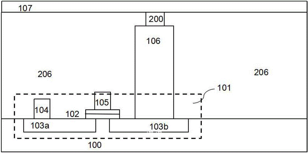
[0041] figure 1 It is the structure diagram of STT-MRAM storage unit. Contains a transistor 101 and MTJ unit 200 . Transistor 101 is built on substrate 100 and includes source 103 a , drain 103 b and gate stack 102 . The gate stack 102 is connected to the word line 105 , the drain 103 b is in drain contact with the MTJ unit 200 through the metal line 106 , and the source 103 a is in source contact with the source node region 104 . MTJ cell 200 is connected to word line 107 . The MTJ unit 200 is formed by adding a tunnel layer between the pinned layer and the free layer, and is perpendicular to the upper plane of the metal line 106 .

[0042] Various technical descriptions related to this show that the preparation of MTJ units can be achieved by conformal deposition techniques, such as atomic layer deposition (ALD) to prepare MTJ unit structures. Figure 1-2 The detailed structure of the invention related to the magnetic recording element is disclosed. The first part of th...

Embodiment 2

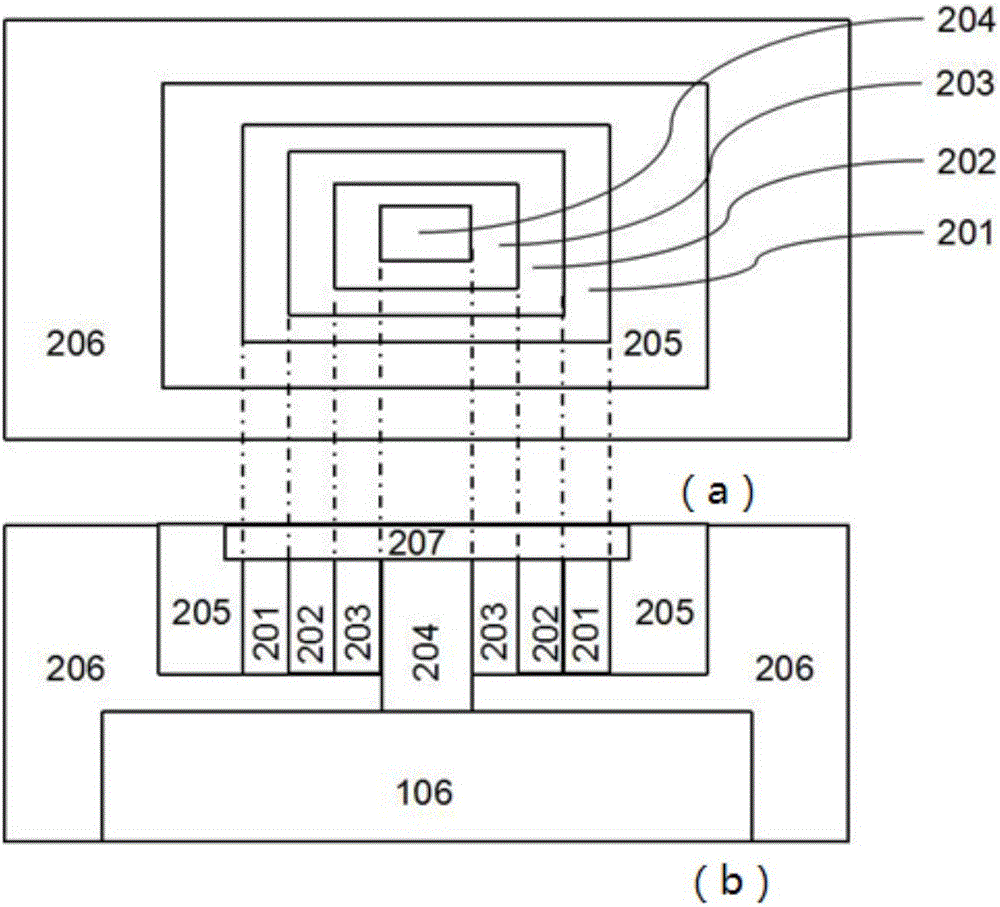
[0047] Figure 14 It is another three-dimensional STT-MRAM memory cell structure diagram. Contains a transistor 101 and MTJ unit 200 . The transistor structure is the same as that of Embodiment 1. Partial adjustments are made at the MTJ unit 200: the corresponding structure of the MTJ is changed from inside to outside into internal electrodes, free layers, barrier layers, pinning layers and external electrodes. The materials used in each layer structure and the preparation method are similar to those in Example 1. The specific structure of its MTJ is as follows Figure 15 shown.

[0048] Two preparation methods of the inner electrode 204 of the MTJ200.

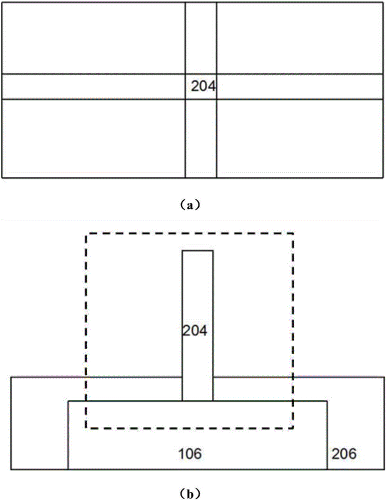
[0049] The first preparation method uses ion beam etching or electron beam etching to directly prepare the internal electrode 204 on 106, such as Figure 16 , 17 shown. Re-utilization of magnetron sputtering or atomic layer deposition (ALD) in Figure 17 Prepare a layer of insulating medium 206 on the basis of Figur...


PUM

PropertyMeasurementUnit
Thicknessaaaaaaaaaa
Thicknessaaaaaaaaaa
Thicknessaaaaaaaaaa

Abstract

The invention discloses an STT-MRAM storage unit. The STT-MRAM storage unit comprises a transistor and an MTJ unit, wherein the transistor is arranged on a substrate, and a drain electrode of the transistor is in drain contact with the MTJ unit through a metal wire; the MTJ unit comprises an inner electrode, and a seed layer, a ferromagnetism pinning layer, a non-magnetic barrier layer, a ferromagnetism free layer and an outer electrode which are wrapped on the periphery of the inner electrode; the metal wire is connected with the inner electrode; the seed layer, the ferromagnetism pinning layer, the non-magnetic barrier layer, the ferromagnetism free layer and the outer electrode are not parallel to a plane where the substrate is respectively; and the seed layer, the ferromagnetism pinning layer, the non-magnetic barrier layer, the ferromagnetism free layer and the outer electrode are arranged at intervals with the metal wire. Through the setting form of the MTJ unit in the STT-MRAM storage unit, the thermal stability factor delta is weakened into linear change along with the square change relation of the original plane structure dimensions, so that the thermal stability factor delta can be compensated by using height, and MTJ miniaturization is facilitated. According to the STT-MRAM storage unit, the space can be effectively utilized, high heat stability is guaranteed, the storage density is improved, various storage modes are provided, and the STT-MRAM storage unit has application prospect for storage devices below 20 nm technology nodes.

Description

technical field [0001] The present invention relates to the technical field of STT-MRAM (Spin Transfer Torque-Magnetic Random AccessMemory, spin transfer torque-magnetic random access memory) memory devices, in particular to a magnetic tunnel junction (Magnetic Tunnel Junction, MTJ) structure and preparation of STT-MRAM devices method. Background technique [0002] Magnetic random access memory (MRAM) is an advanced storage technology that can replace traditional memory. It has good non-volatility, that is, the data will not be lost after power failure, good thermal stability, the stored information can be stored for more than ten years, and good read and write stability, the read and write times can reach 10 16 Second-rate. The early MRAM uses current to generate an external magnetic field to change the magnetic state of the free layer. Due to the large write current required and high energy consumption, miniaturization is limited. The spin-transfer torque magnetic rando...

Claims


Application Information

Patent Timeline
IPC IPC(8): H01L27/115
CPCH10B53/20H10B53/30H10B69/00
Inventor 王真何岳巍胡少杰闵泰
Owner XI AN JIAOTONG UNIV
Why Eureka
Try Eureka