Photoelectric detector with adjustable response spectrum

A photodetector and adjustable technology, which is applied in the direction of circuits, electrical components, semiconductor devices, etc., can solve the problems of inability to detect spectral resolution and non-adjustable response spectrum, and achieve dynamic adjustment, miniaturization and chip-based effects

Active Publication Date: 2017-05-31
SOUTHEAST UNIV
View PDF8 Cites 21 Cited by
  • Summary
  • Abstract
  • Description
  • Claims
  • Application Information

AI Technical Summary

Problems solved by technology

[0005] Purpose of the invention: In order to overcome the shortcomings of the existing photodetector devices, which have a fixed and non-adjustable response spectrum, and cannot achieve spectral resolution detection alone, they must be combined with other optical components or systems

Method used


Image

  • Photoelectric detector with adjustable response spectrum
  • Photoelectric detector with adjustable response spectrum
  • Photoelectric detector with adjustable response spectrum

Examples


Embodiment Construction

[0021] The present invention will be further described below in conjunction with the accompanying drawings.

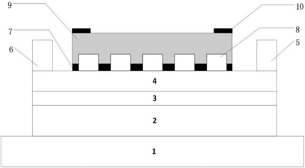
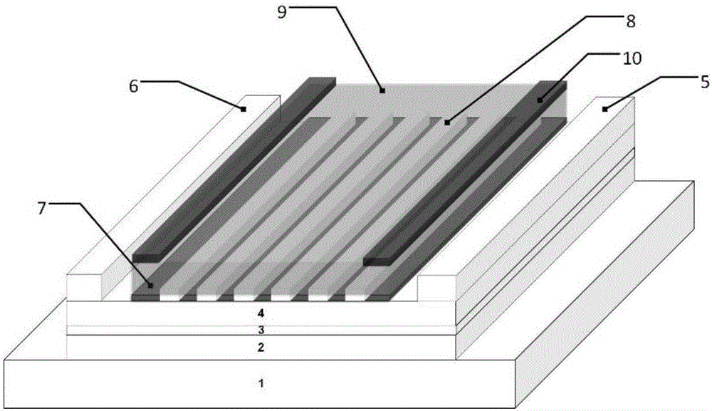
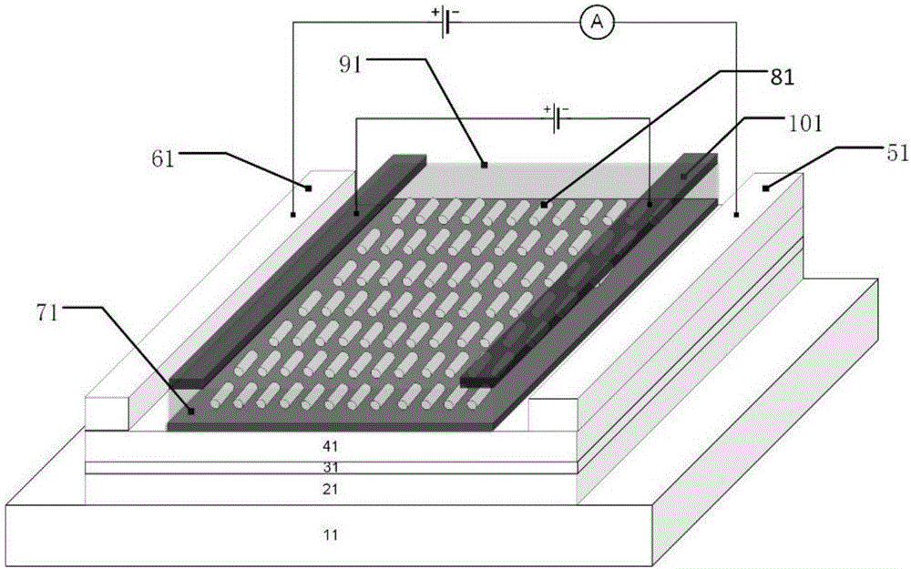
[0022] figure 1 It is a schematic diagram of the cross-sectional structure of the present invention. Such as figure 1 As shown, the structure of the novel photodetector with adjustable response spectrum of the present invention includes an insulating substrate 1 , a metal gate 2 , a first insulating isolation layer 3 and a semiconductor layer 4 from bottom to top. A second insulating isolation layer 7, a plasmonic metal nanostructure 8, a metal source 5 and a metal drain 6 are provided on the semiconductor layer 4; an electro-optic crystal covering layer 9 is provided on the second insulating isolation layer 7, and Two transparent lead-out electrodes are arranged on both sides above the electro-optic crystal covering layer as electrodes of an external circuit, and are connected with the external circuit. A second insulating layer 7 is provided between the semiconduc...


PUM


Abstract

The invention provides a novel photoelectric detector with adjustable response spectrum. The novel photoelectric detector is characterized in that the device structure sequentially comprises an insulation substrate, a gate, a first insulation isolation layer, a conductive channel layer, a metal source-drain, a second insulation isolation layer, a plasmon metal nanometer structure, an electro-optical crystal coverage layer and a transparent leading-out electrode from bottom to top. The refractive index of the electro-optical crystal coverage layer is controlled by an externally-applied voltage, so that the refractive index of a coverage substance is changed with the change of the external voltage to further control plasmon resonant wavelength of the metal nanometer structure and response wavelength of the detector. In the detector device structure, the spectrum can be regulated by the voltage, miniaturization and microminiaturization are facilitated, and the novel photoelectric detector has good application prospect in the field of a photoelectric device and optical communication.

Description

technical field [0001] The invention relates to a novel photodetection device with adjustable response spectrum, which can be used to dynamically adjust the response spectrum range of the photodetector. Background technique [0002] As a device that converts optical signals into electrical signals, photodetectors have been used in many fields. The traditional internal photoelectric effect photodetection device is based on the semiconductor energy band theory, as long as the incident photon energy is greater than the forbidden band width of the semiconductor material, it can excite valence band electrons to the conduction band, form photoinduced carriers, generate photocurrent, and realize photodetection. However, most of the photoelectric detection based on this principle is a wide spectral band for detection, and the mechanism cannot achieve fine resolution of the spectrum, and once the semiconductor material is determined, the adjustment of the response spectrum cannot be ...

Claims


Application Information

Patent Timeline
IPC IPC(8): H01L31/0232H01L31/113B82Y40/00
CPCB82Y40/00H01L31/02327H01L31/1136
Inventor 王琦龙陈广甸翟雨生
Owner SOUTHEAST UNIV
Why Eureka
Try Eureka