
PIN structure graphene photodetector with adjustable Fermi level and preparation method thereof

A Fermi level and photodetector technology, which is applied in sustainable manufacturing/processing, semiconductor devices, climate sustainability, etc., can solve problems such as low absorption rate and slow response speed, so as to improve the signal-to-noise ratio of devices, Effect of reducing dark current and enhancing responsivity

Active Publication Date: 2017-05-31
UNIV OF ELECTRONIC SCI & TECH OF CHINA
View PDF6 Cites 3 Cited by
  • Summary
  • Abstract
  • Description
  • Claims
  • Application Information

AI Technical Summary

Problems solved by technology

[0004] The purpose of the present invention is to address the deficiencies in the prior art, to provide a PIN structure graphene photodetector with adjustable Fermi energy level and its preparation method, the PIN structure graphene photodetector with adjustable Fermi energy level and Its preparation method can solve the problems of low absorption rate and slow response speed of graphene as a photodetector material

Method used


Image

  • PIN structure graphene photodetector with adjustable Fermi level and preparation method thereof
  • PIN structure graphene photodetector with adjustable Fermi level and preparation method thereof
  • PIN structure graphene photodetector with adjustable Fermi level and preparation method thereof

Examples


Embodiment Construction

[0023] In order to make the purpose, technical solution and advantages of the present application clearer, the present application will be further described in detail below in conjunction with the accompanying drawings and specific embodiments.

[0024] For simplicity, some technical features known to those skilled in the art are omitted from the following description.

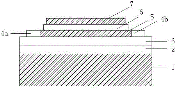
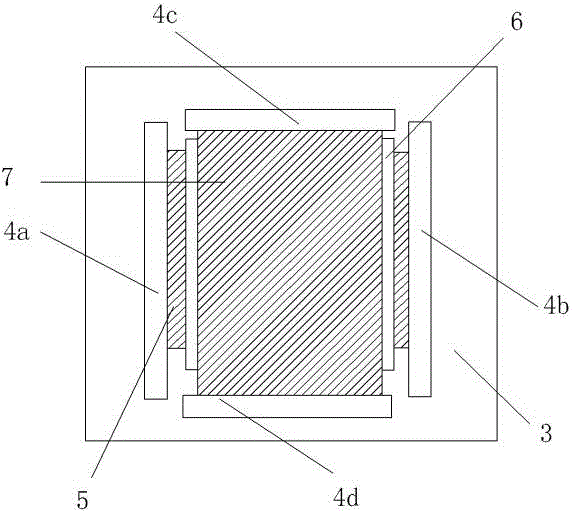
[0025] According to one embodiment of the present application, a kind of PIN structure graphene photodetector with adjustable Fermi level is provided, such as figure 1 , 2 As shown, there are substrate 1, metal layer 2, insulating layer 3, first graphene layer 5, dielectric layer 6 and second graphene layer 7 from bottom to top, and the gate voltage is applied to the metal layer 2 during use. The insulating layer 3 has a source electrode 4a, a drain electrode 4b and a first electrode 4c, generally one-time can complete the making of 4 electrodes, except the source electrode 4a, drain electrode 4b and first el...


PUM

PropertyMeasurementUnit
Thicknessaaaaaaaaaa
Thicknessaaaaaaaaaa

Abstract

The invention relates to the field of graphene photodetectors, in particular to a PIN structure graphene photodetector with adjustable Fermi level and a preparation method thereof; the PIN structure graphene photodetector with adjustable Fermi level comprises a substrate, a metal layer, an insulating layer, a P-doped graphene layer, a dielectric layer and an N-doped graphene layer sequentially from bottom to top; gate voltage is applied to the metal layer; the insulating layer has a source electrode, a drain electrode and a first electrode, and the source electrode and the drain electrode are arranged on two sides of the first graphene layer respectively and are both connected to the first graphene layer; the first electrode and the second electrode are arranged on two sides of the second graphene layer respectively, and the first electrode is connected to the second graphene layer; the P-doped graphene layer, the dielectric layer and the N-doped graphene layer form a PIN structure; the first graphene layer, the source electrode, the drain electrode, the insulating layer and the metal layer form a field-effect transistor. The field-effect transistor made with graphene material is combined with the PIN structure to form the photodetector, providing high-response quick detection under ultraviolet-to-infrared broad band.

Description

technical field [0001] The invention relates to the field of graphene photodetectors, in particular to a PIN-structure graphene photodetector with adjustable Fermi energy level and a preparation method thereof. Background technique [0002] Graphene (Grahpene) is a new carbonaceous material that is tightly packed into a two-dimensional honeycomb lattice structure by a single layer of carbon atoms. It has excellent mechanical, electrical, thermal and optical properties. Since 2004, the team of Novoselov and Geim Since single-layer graphene at room temperature was prepared by mechanical exfoliation, it has gradually become a research hotspot. Graphene is undoubtedly the thinnest known material, with a single layer of graphene only 0.3 nanometers thick (one carbon atom thick), but it is also the hardest nanomaterial. Graphene can absorb 2.3 percent of white light, much higher than other allotropes of carbon. Graphene can observe the Hall effect at room temperature. Graphene ...

Claims


Application Information

Patent Timeline
IPC IPC(8): H01L31/09H01L31/18H01L31/0216H01L31/0232
CPCH01L31/02161H01L31/02327H01L31/09H01L31/18Y02P70/50
Inventor 王军潘锐李凯苟君蒋亚东
Owner UNIV OF ELECTRONIC SCI & TECH OF CHINA
Learn More