
Epitaxial structure of AlInGaN-based multi-quantum well light-emitting diode

A technology of light-emitting diodes and epitaxial structures, applied in electrical components, circuits, semiconductor devices, etc., can solve problems such as difficulty in ensuring the quality of quantum barrier materials, failure to achieve the design effect, and decline in LED efficiency, so as to reduce electron leakage and improve efficiency Dip effect, effect of improving electron-hole matching degree

Pending Publication Date: 2017-05-31
NANCHANG UNIV +1
View PDF4 Cites 2 Cited by
  • Summary
  • Abstract
  • Description
  • Claims
  • Application Information

AI Technical Summary

Problems solved by technology

As a non-radiative recombination, its rate is proportional to the cube of the carrier concentration; as the carrier concentration increases, Auger recombination will gradually dominate, resulting in a decrease in LED efficiency
(2 electron leakage
However, this design must at the same time ensure that the quantum barrier has a high enough barrier height to confine carriers, which requires the design of the quantum barrier to find the best point between the improvement of lattice matching and the reduction of forbidden band width; Therefore, the quantum barrier material is often designed as a high Al and high In material. In the actual material growth process, it is difficult to ensure the quality of the quantum barrier material and cannot achieve the designed effect.

Method used


Image

  • Epitaxial structure of AlInGaN-based multi-quantum well light-emitting diode
  • Epitaxial structure of AlInGaN-based multi-quantum well light-emitting diode
  • Epitaxial structure of AlInGaN-based multi-quantum well light-emitting diode

Examples


Embodiment 1

[0025] This embodiment takes the silicon substrate InGaN / GaN multi-quantum well LED material structure as an example.

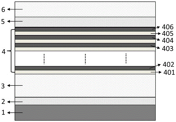
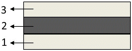
[0026] refer to figure 1 . Clean a Si(111) substrate 1; put it into MOCVD to grow an aluminum nitride transition layer 2; grow an N-type gallium nitride 3 with a thickness of 2.4 μm on the aluminum nitride transition layer 2; 9 cycles of In grown on 3 0.16 Ga 0.84 N (3nm thick) / GaN (10nm thick) multi-quantum well light-emitting active layer 4; the structure of the n-1th quantum barrier 404 in the multi-quantum well is as follows image 3 As shown, the thickness of the GaN / AlGaN / GaN layer is 2.5nm / 5nm / 2.5nm, and the Al composition is 20%. An AlGaN electron blocking layer 5 with a thickness of 20 nm and a P-type gallium nitride layer 6 with a thickness of 100 nm are grown successively on the light emitting active layer 4 . The growth process of all layers adopts conventional growth methods.

Embodiment 2

[0028] Compared with Example 1, the AlGaN of the n-1th quantum barrier 404 in the multi-quantum luminescent active layer 4 is changed to AlInGaN, the Al composition is 30%, and the In composition is 10%.

Embodiment 3

[0030] Compared with Example 1, the structure of the n-1th quantum barrier 404 in the multi-quantum light-emitting active layer 4 is as follows image 3 As shown, the thickness of the AlGaN / GaN / AlGaN layer is 3nm / 4nm / 3nm; along the growth direction, the Al composition of the first layer of AlGaN is 20%, and the Al composition of the second layer of AlGaN is 15%.


PUM

PropertyMeasurementUnit
Thicknessaaaaaaaaaa
Thicknessaaaaaaaaaa

Abstract

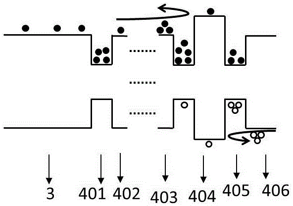
The invention discloses an epitaxial structure of an AlInGaN-based multi-quantum well light-emitting diode. The epitaxial structure comprises a substrate and a GaN-based semiconductor lamination layer, wherein the substrate is used for material growing, the GaN-based semiconductor lamination layer is laminated on the substrate and at least comprises an N-type AlInGaN-based semiconductor layer, a P-type AlInGaN-based semiconductor layer and a multi-quantum well light-emitting active layer, and the multi-quantum well light-emitting active layer is sandwiched between the N layer and the P layer, the AlInGaN-based multi-quantum well light-emitting diode is characterized in that in the multi-quantum well light-emitting active layer, the forbidden bandwidth of a quantum barrier previous to an n(th) quantum well or a quantum barrier previous to an (n-1)th quantum well or a quantum barrier previous to the n(th) / (n-1)th quantum well is larger than the forbidden bandwidths of other quantum barriers. By the epitaxial structure, the barriers of electrons injected to main light-emitting wells are improved, the barriers of holes overflowing out of the main light-emitting wells are simultaneously improved, the electron and hole matching degree in the main light-emitting wells can be improved, electron leakage is reduced, an efficiency suddenly-reduced effect is improved, so that the quantum efficiency of a light-emitting diode (LED) is improved.

Description

technical field [0001] The invention relates to the technical field of semiconductor lighting, in particular to an epitaxial structure of an AlInGaN-based multi-quantum well light-emitting diode. Background technique [0002] With the continuous development and improvement of material growth and device technology level, the photoelectric properties of InGaN / GaN multi-quantum well light-emitting diodes (LEDs) have made breakthroughs, making them gradually used in instrument work instructions, traffic lights, large-screen displays, lighting and other fields. However, although great progress has been made, GaN-based LEDs still have many problems, which hinder their further popularization and application. As the current density increases, the phenomenon that the internal quantum efficiency (IQE) of the LED decreases sharply is one of the most important problems, and this phenomenon is called the IQE dip effect. There are many studies on the causes of GaN-based LED efficiency d...

Claims


Application Information

Patent Timeline
IPC IPC(8): H01L33/06H01L33/32
CPCH01L33/06H01L33/32
Inventor 莫春兰全知觉江风益陶喜霞刘军林王光绪
Owner NANCHANG UNIV
Learn More