Groove-type low-barrier schottky diode and manufacturing method

A Schottky diode, trench technology, used in semiconductor/solid-state device manufacturing, electrical components, circuits, etc., can solve problems such as increased leakage current, and achieve enhanced surge capability, superior high voltage resistance, and reduced potential barriers. Effect

Inactive Publication Date: 2018-06-22
BEIJING CENTURY GOLDRAY SEMICON CO LTD
View PDF5 Cites 17 Cited by
  • Summary
  • Abstract
  • Description
  • Claims
  • Application Information

AI Technical Summary

Problems solved by technology

However, the reverse bias leakage current will also increase after the potential barrier is lowered. How to maintain high voltage and high temperature characteristics while reducing the potential barrier is the key to research

Method used


Image

  • Groove-type low-barrier schottky diode and manufacturing method
  • Groove-type low-barrier schottky diode and manufacturing method
  • Groove-type low-barrier schottky diode and manufacturing method

Examples


Embodiment Construction

[0033] The present invention will now be described more fully with reference to the accompanying drawings, in which exemplary embodiments of the invention are shown. This invention may, however, be embodied in many different forms and should not be construed as limited to the exemplary embodiments set forth herein. Rather, these embodiments are provided so that this disclosure will be thorough and complete, and will fully convey the scope of the invention to those skilled in the art.

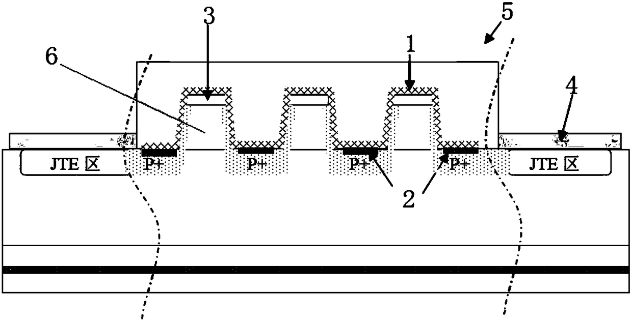
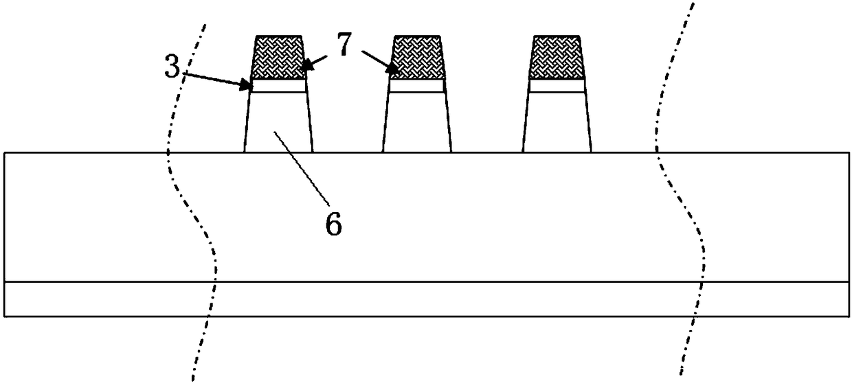
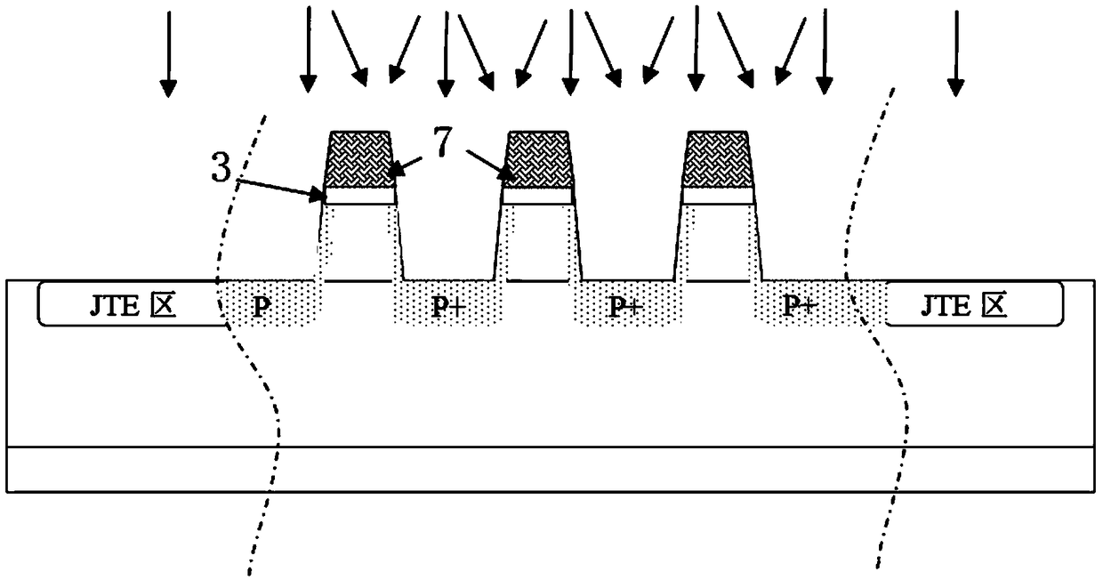
[0034] The invention reduces the Schottky contact potential barrier of the device by improving the device structure and process without changing the Schottky contact metal, and finally reduces the forward voltage drop and conduction loss of the device.

[0035] On the SiC substrate of the first conductivity type, a buffer layer of the first conductivity type is epitaxially, the thickness of the buffer layer is between 0.5-2 μm, and the concentration is 1E18cm -3 Left and right; epitaxial drift ...


PUM


Abstract

The invention discloses a groove-type low-barrier schottky diode and a manufacturing method. The active area of the schottky diode is a groove structure. The top of a bench surface is a schottky contact. The side wall of the bench surface and a groove bottom are highly-doped p-type areas which are electrically connected. A p-type ohmic contact is formed on the groove bottom. The depth of a grooveis dt and a width is Wt. The width of the bench surface is Wm. The junction depth of each p-type area is dp. The Wt is greater than 1 micron, the Wm is greater than 0.5 micron, the dt is greater than0.5 micron and the dp is greater than 0.5 micron. In the invention, a mirror image force barrier reduction method is used to form the low-barrier schottky contact on the bench surface. P+ doping and the ohmic contact are performed on the side wall of the bench surface and the groove bottom so as to form parallel pn diodes. The surge capacity of a device is enhanced, simultaneously, a schottky conductive channel is shielded, and the voltage endurance capability and the high temperature resistance capability of the device are increased. By using the schottky diode, the barrier of the device canbe reduced, simultaneously, the excellent voltage endurance capability, a high temperature resistance characteristic and the surge capability are maintained.

Description

technical field [0001] The invention relates to the field of semiconductors, in particular to a trench type low potential barrier Schottky diode and a preparation method thereof. Background technique [0002] Since the Schottky diode is a unipolar device, there is almost no reverse recovery current, and it has better reverse recovery characteristics than the pn diode. Schottky diodes of wide bandgap semiconductor silicon carbide (SiC) can withstand voltages above 3300V, and have better advantages in high-voltage and high-frequency switching circuits. However, also due to the wide bandgap characteristics of silicon carbide materials, the potential barriers of SiC Schottky diodes are generally relatively high. For example, the potential barriers of Ti and MO commonly used in the industry are between 1.2-1.3eV, while the potential barriers of Ni and Pt The barrier is larger than 1.6eV. A high potential barrier can make the device withstand higher withstand voltage and high te...

Claims


Application Information

Patent Timeline
Patent Type & Authority Applications(China)
IPC IPC(8): H01L29/872H01L29/45H01L29/47H01L29/06H01L21/329
CPCH01L29/0684H01L29/45H01L29/47H01L29/6606H01L29/872
Inventor 倪炜江徐妙玲李明山
Owner BEIJING CENTURY GOLDRAY SEMICON CO LTD
Why Eureka
Try Eureka