Dual-frequency wideband wave absorber

An absorber and broadband technology, which is applied in the field of dual-frequency broadband absorbers, can solve the problems of narrow absorbing bandwidth, increasing the section size of absorbing structural units, and small application range of dual-frequency absorbing, so as to achieve a wide absorbing bandwidth. , The effect of short preparation cycle and low cost

Pending Publication Date: 2017-05-31
UNIV OF ELECTRONIC SCI & TECH OF CHINA
View PDF8 Cites 13 Cited by
  • Summary
  • Abstract
  • Description
  • Claims
  • Application Information

AI Technical Summary

Problems solved by technology

However, this approach has several disadvantages. First, the absorption bandwidth of the resonant structure is extremely narrow; second, the patchwork of absorbing structural units with different resonant frequencies will increase the cross-sectional size of the entire absorbing structural unit.

Method used


Image

  • Dual-frequency wideband wave absorber
  • Dual-frequency wideband wave absorber

Examples


Embodiment Construction

[0017] In order to make the object of the present invention, the technical problem to be solved and the technical solution clearer, the present invention will be further described below in conjunction with the accompanying drawings and specific embodiments.

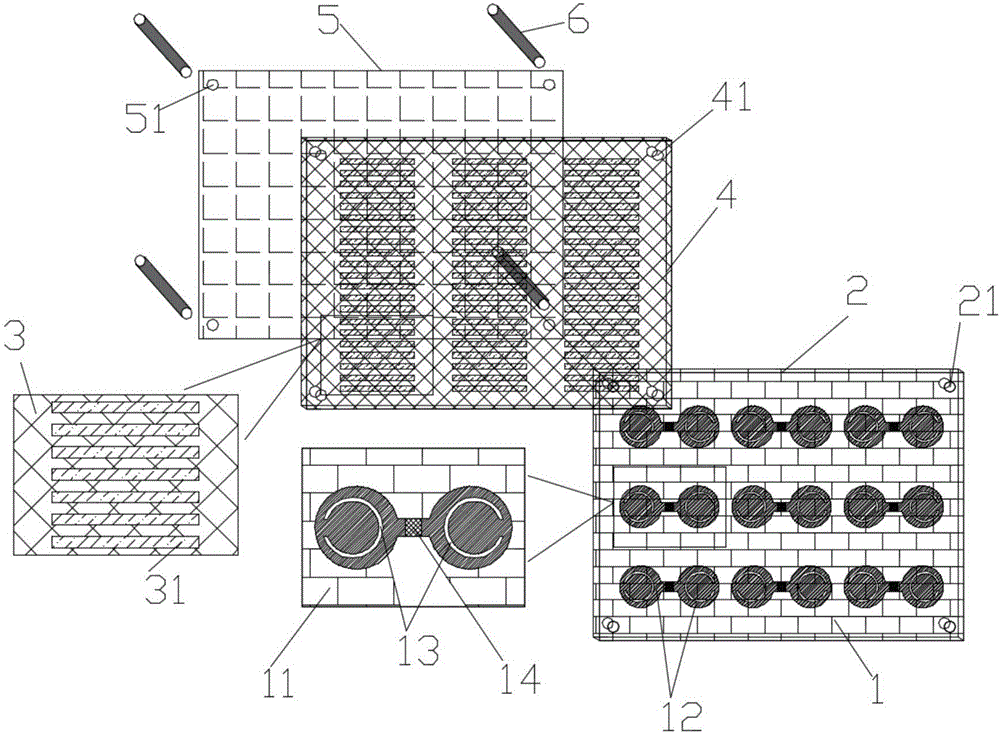
[0018] figure 1 It is an overall development schematic diagram of the present invention, including a periodic wave-absorbing surface structure 1, a first-layer dielectric substrate 2, a periodic frequency-selective surface structure 3, a second-layer dielectric substrate 4, a metal shielding floor 5 and a The plastic screw 6 of the layer dielectric substrate 2 and the second layer dielectric substrate 4 . The periodic wave-absorbing surface structure 1 is composed of a plurality of wave-absorbing structural units 11 printed on the first layer of dielectric substrate 2 (dielectric constant 2.65, loss tangent 0.002) with a thickness of 1mm along the horizontal and vertical directions. Two-dimensional periodic arrangement; ...


PUM


Abstract

The invention discloses a dual-frequency wideband wave absorber, which comprises a periodic wave absorption surface structure, a first layer medium base plate, a periodic frequency selection surface structure, a second layer medium base plate, a metal shielding floor and plastic screws used for connecting the first layer medium base plate and the second layer medium base plate, wherein the periodic wave absorption surface structure is printed on the first layer medium base plate and consists of two metal round sheets, two opening resonant rings and wave absorption structure units; the two metal round sheets are symmetrical at the left side and the right side; the two opening resonant rings are symmetrical at the left side and the right side; the wave absorption structure unit is welded between the two metal round sheet arms. The periodic frequency selection surface structure is formed by a plurality of metal resonant units printed on the second layer medium base plate. The metal shielding floor is printed on the back side of the second layer medium base plate. The opening resonant rings and the metal resonant units simultaneously act to realize the reflection characteristics in a certain frequency band range, so that the double-frequency wideband sound absorption is formed. The wave absorption band width and the wave absorption rate can be changed through regulating the distance between the first layer medium base plate and the second layer medium base plate.

Description

technical field [0001] The invention belongs to the technical field of microwave absorbing materials, and relates to a dual-frequency broadband absorber. Background technique [0002] With the rapid development of wireless communication, the electromagnetic environment in space is becoming more and more complex. These random electromagnetic waves scattered in space will cause interference to wireless communication and greatly reduce the quality of communication. The use of absorbing materials can reduce or even eliminate the interference of complex electromagnetic environments on wireless communications. Dual-frequency broadband communications in wireless systems require the use of corresponding multi-frequency broadband absorbing materials. Therefore, the research on dual-frequency broadband microwave absorption is a hot and difficult point in the academic circles and even in the industrial circles. [0003] In order to achieve dual-band wave-absorbing characteristics, the...

Claims


Application Information

Patent Timeline
IPC IPC(8): H01Q17/00
CPCH01Q17/008Y02D30/70
Inventor 林先其梅鹏张鹏程于家伟王旭姜励勤蔡杨沈奕同刘南枫
Owner UNIV OF ELECTRONIC SCI & TECH OF CHINA
Why Eureka
Try Eureka