Auxiliary power supply unit for trams
A technology of auxiliary power supply and electric vehicle, which is applied to electric devices, output power conversion devices, electric vehicles, etc., can solve the problem of no power storage, and achieve the effect of suppressing damage and preventing large currents from flowing through switching elements.
- Summary
- Abstract
- Description
- Claims
- Application Information
AI Technical Summary
Problems solved by technology
Method used
Image
Examples
Embodiment approach 1
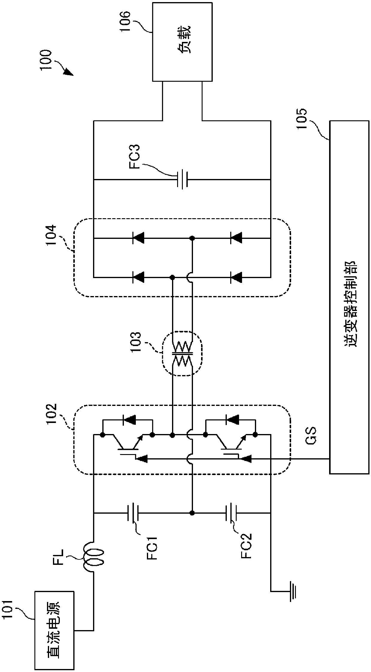
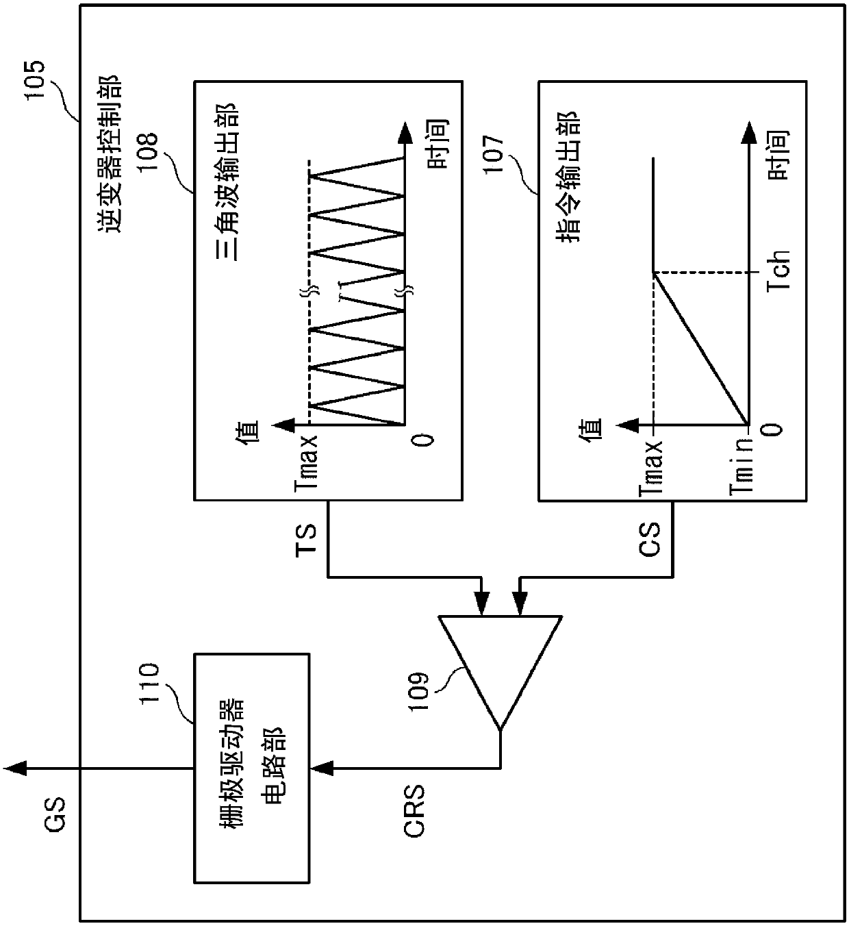
[0044] The electric vehicle auxiliary power supply device (hereinafter also simply referred to as "auxiliary power supply device") 100 according to Embodiment 1 of the present invention is as follows: figure 1As shown, it includes: an inverter circuit section 102 that converts DC power input from a DC power supply 101 into AC power; a primary coil that inputs AC power from the inverter circuit section 102, and a secondary coil that is insulated from the primary coil, and A transformer 103 that outputs alternating current from the secondary coil; a converter circuit section 104 that converts the alternating current output from the transformer 103 into direct current; a smoothing capacitor FC3 for smoothing the direct current voltage output from the converter circuit section 104; and the output The inverter control unit 105 of the gate signal GS to operate the switching elements of the inverter circuit unit 102 .
[0045] As shown in the same drawing, the inverter circuit unit 1...
Deformed example 1
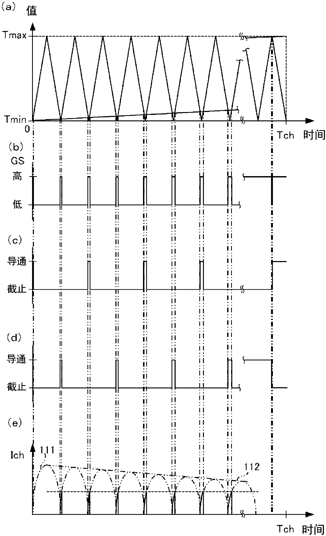
[0105] The minimum value Tmin may be a value between zero and Vmin at which the pulse width of the gate signal GS first output from the gate driver circuit unit 110 in the charge mode becomes the minimum response time of the switching element.
[0106] By setting the minimum value Tmin to a value between zero and Vmin, the current output from the inverter circuit unit 102 after the inverter control unit 105 starts operating in the charging mode can be made close to that of the inverter. The minimum value that the circuit unit 102 can output. Accordingly, it is possible to reduce the current flowing through the switching element at the initial stage of charging of the smoothing capacitor FC3 in which a particularly large current is likely to flow through the switching element.
[0107] As a result, even if the timing of outputting current from the inverter circuit unit 102 varies, or the pulse width of the gate signal GS varies, it is possible to suppress excessive switching el...
Deformed example 2
[0110] The number of elements constituting the inverter circuit unit 102 and the converter circuit unit 104 and their connection methods can be appropriately changed. Correspondingly, the number and connection method of the filter capacitors FC1 and FC2 can also be appropriately changed. The number of filter capacitors FC3 can also be appropriately changed.
PUM
 Abstract
Description
Claims
Application Information


