Focal plane detection apparatus, focal plane calibration method and silicon chip aeration method

A technology of detection device and calibration method, which is used in testing optical performance, microlithography exposure equipment, photolithography process exposure device, etc., can solve actual focal plane drift, calibration and compensation of optimal focal plane offset, height and problems such as tilt deviation, to achieve the effect of good measurement accuracy and measurement repeatability

Active Publication Date: 2017-06-09
SHANGHAI MICRO ELECTRONICS EQUIP (GRP) CO LTD
View PDF4 Cites 15 Cited by
  • Summary
  • Abstract
  • Description
  • Claims
  • Application Information

AI Technical Summary

Problems solved by technology

[0003] However, the above measurement method faces the following problem: because the projection objective lens 1 is affected by processing, assembly, or external environment such as temperature and air pressure, the actual focal plane drifts, so the best focal plane of the projection objective lens 1 always exists relative to the FLS zero plane A certain height and inclination deviation
[0004] It can be seen from this that this type of measurement method for finding the best focal plane requires many steps in operation and execution, and the measurement and calibration must be completed through multiple process experiments. Therefore, how to quickly and accurately measure the offset of the best focal plane Calibration and compensation is a technical problem to be solved urgently by those skilled in the art

Method used


Image

  • Focal plane detection apparatus, focal plane calibration method and silicon chip aeration method
  • Focal plane detection apparatus, focal plane calibration method and silicon chip aeration method
  • Focal plane detection apparatus, focal plane calibration method and silicon chip aeration method

Examples


Embodiment 1

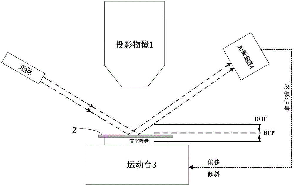
[0034] Such as image 3 As shown, this embodiment provides a focal plane detection device, including: a light source unit (not shown in the figure), an imaging unit, a focusing drive unit 109, a moving stage unit 107, and a control unit 110, wherein the light source unit It is used to irradiate the mask plate 101 to generate an imaging beam, and the mask plate 101 has a focusing pattern 101a; the imaging unit is used to image the focusing pattern 101a on the reflection device 108 and the focusing image sensor 106; The focusing drive unit 109 is used to vertically adjust the projection objective lens 104 to complete the focusing; the moving table unit 107 is provided with a reflecting device 108 with a reflecting mark 108a, which is used to move the reflecting device 108 horizontally and vertically The control unit 110 is used to analyze and process the graphic data collected by the focusing image sensor 106 , and to control the focusing drive unit 109 in feedback.

[0035] Sp...

Embodiment 2

[0055] Such as Figure 9 As shown, the focusing drive unit 109 in this embodiment adopts a vertical displacement adjustment platform with a vertical focusing function, and the control unit 110 is directly connected to the vertical displacement adjustment platform, and the output focusing control amount is directly The vertical displacement adjustment table is endowed, and the vertical displacement adjustment table is used as the actuator to complete the precise displacement action of the vertical position of the silicon wafer. In other words, the motion table unit 107 in this embodiment only moves the reflection device 108 horizontally.

Embodiment 3

[0057] Such as Figure 10 As shown, in this embodiment, a physical mask is used to replace the digital mask in Embodiment 1, and the physical mask is a transmissive or reflective mask 101, which is carried by the mask table 101b. The focusing pattern 101a on the physical mask is an IC integrated circuit process pattern to be exposed and developed, and this pattern can be analyzed and processed by a specific focusing algorithm and an image processing system of the control unit 110 .

[0058] In summary, the focal plane detection device of the present invention includes: a light source unit for irradiating the mask 101 to generate an imaging beam; an imaging unit for imaging the focusing pattern 101a on the mask 101 into a focusing image On the sensor 106; the focusing drive unit 109 is used to vertically adjust the projection objective lens 104 or the moving stage unit 107 to complete focusing; the moving stage unit 107 is provided with a reflective device 108 with a reflective...


PUM


Abstract

The invention discloses a focal plane detection apparatus, a focal plane calibration method and a silicon chip aeration method. The focal plane detection apparatus comprises a light source unit, an imaging unit, a focus adjusting drive unit, a movement platform unit and a control unit, wherein the light source unit is used for illuminating a mask plate to generate an imaging beam; the imaging unit is used for imaging a focus adjusting pattern on the mask plate onto a focus adjusting image sensor; the focus adjusting drive unit is used for vertically adjusting a projection objective or the movement platform unit to complete the focus adjustment; the movement platform unit is provided with a reflection apparatus with a reflective marker, and the movement platform unit is used for moving the reflection apparatus to a position right below the projection objective; and the control unit is used for analyzing and processing graphic data acquired by the focus adjusting image sensor and controlling the focus adjusting drive unit. By adopting the focal plane detection apparatus, the focal plane calibration method and the silicon chip aeration method, an optimum focal plane offset can be rapidly and accurately calibrated and compensated.

Description

technical field [0001] The invention relates to the field of integrated circuit manufacturing, in particular to a focal plane detection device, a focal plane calibration method and a silicon wafer exposure method. Background technique [0002] During the exposure process of the lithography machine, in order to obtain the best exposure quality, the upper surface of the silicon wafer must always be in the best focal plane of the projection objective. Such as figure 1 As shown, the existing technical means usually measure the position of the upper surface of the silicon wafer 2 by the photodetector 4 in the lithography machine, that is, the focusing and leveling system (FLS, English full name: Focusing and leveling system), and use The adjustment mechanism, that is, the moving table 3 drives the silicon wafer 2 to adjust it to the best focal plane position of the calibrated projection objective lens 1 . [0003] However, the above measurement method faces the following proble...

Claims


Application Information

Patent Timeline
Patent Type & Authority Applications(China)
IPC IPC(8): G03F7/20G01M11/02G03F9/00
CPCG01M11/02G03F7/2002G03F9/00
Inventor 王天寅许琦欣李玉龙
Owner SHANGHAI MICRO ELECTRONICS EQUIP (GRP) CO LTD
Why Eureka
Try Eureka