Semiconductor wafer test method, projection manufacturing method, semiconductor device and electronic device

A technology of wafer testing and manufacturing methods, which is applied in semiconductor devices, semiconductor/solid-state device manufacturing, semiconductor/solid-state device testing/measurement, etc., and can solve problems such as pollution, influence of ball bottom metal layer bump process, and missing bumps , to achieve the effect of avoiding missing bumps

Inactive Publication Date: 2017-06-09
SEMICON MFG INT (SHANGHAI) CORP +1
View PDF5 Cites 1 Cited by
  • Summary
  • Abstract
  • Description
  • Claims
  • Application Information

AI Technical Summary

Problems solved by technology

However, the manufacturing process of high-end chips is very complicated and the yield rate is difficult to control, while the yield rate of the bump manufacturing process is relatively stable. Therefore, in order to save packaging costs, it is usually necessary to perform chip probe testing (CP, chip probing) to screen the wafers and pick out unqualified chips
But when doing CP testing, the probes will come into contact with the pads of the wafer, which may cause damage or contamination of the pads (such as aluminum pads)
At the same time, the test pin marks make the surface of the pad uneven, which makes it difficult to use physical vapor deposition to prepare the bottom metal layer in the subsequent bumping process
The quality of the metal layer at the bottom of the ball has a great impact on the subsequent bumping process, such as figure 1 As shown, the middle part of the aluminum pad in area 100 in the figure is the defect on the surface of the aluminum pad caused by the test needle mark, which makes the surface of the pad uneven, and the metal layer at the bottom of the ball is not deposited well, resulting in missing bumps.

Method used


Image

  • Semiconductor wafer test method, projection manufacturing method, semiconductor device and electronic device
  • Semiconductor wafer test method, projection manufacturing method, semiconductor device and electronic device
  • Semiconductor wafer test method, projection manufacturing method, semiconductor device and electronic device

Examples


Embodiment 1

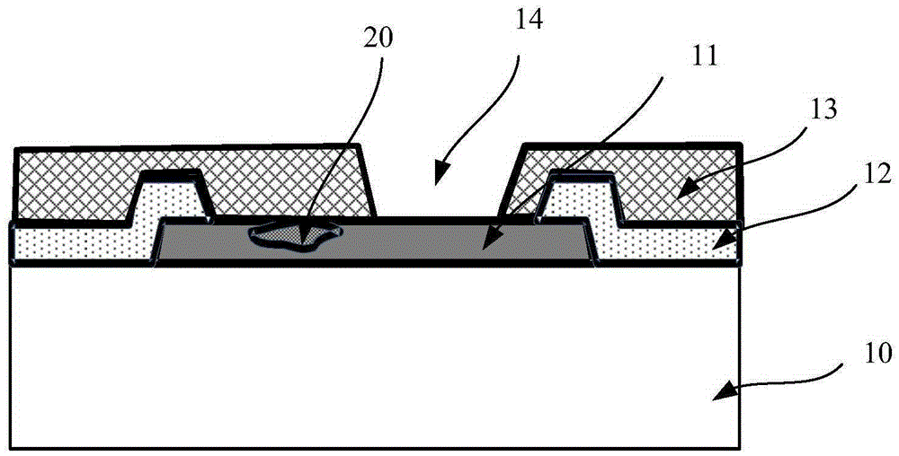
[0032] Below, refer to Figures 4A to 4D and Figure 5 A method for manufacturing wafer bumps according to an embodiment of the present invention will be specifically described. in, Figure 4A to Figure 4D A cross-sectional view of a structure formed in the relevant steps of a wafer bump manufacturing method according to an embodiment of the present invention; image 3 It is a flowchart of a method for manufacturing wafer bumps according to an embodiment of the present invention.

[0033] The method for manufacturing wafer bumps according to Embodiment 1 of the present invention includes the following steps:

[0034] Step S101 , providing a semiconductor wafer, forming bonding pads and a first passivation layer covering the semiconductor wafer and exposing the bonding pads on the semiconductor wafer.

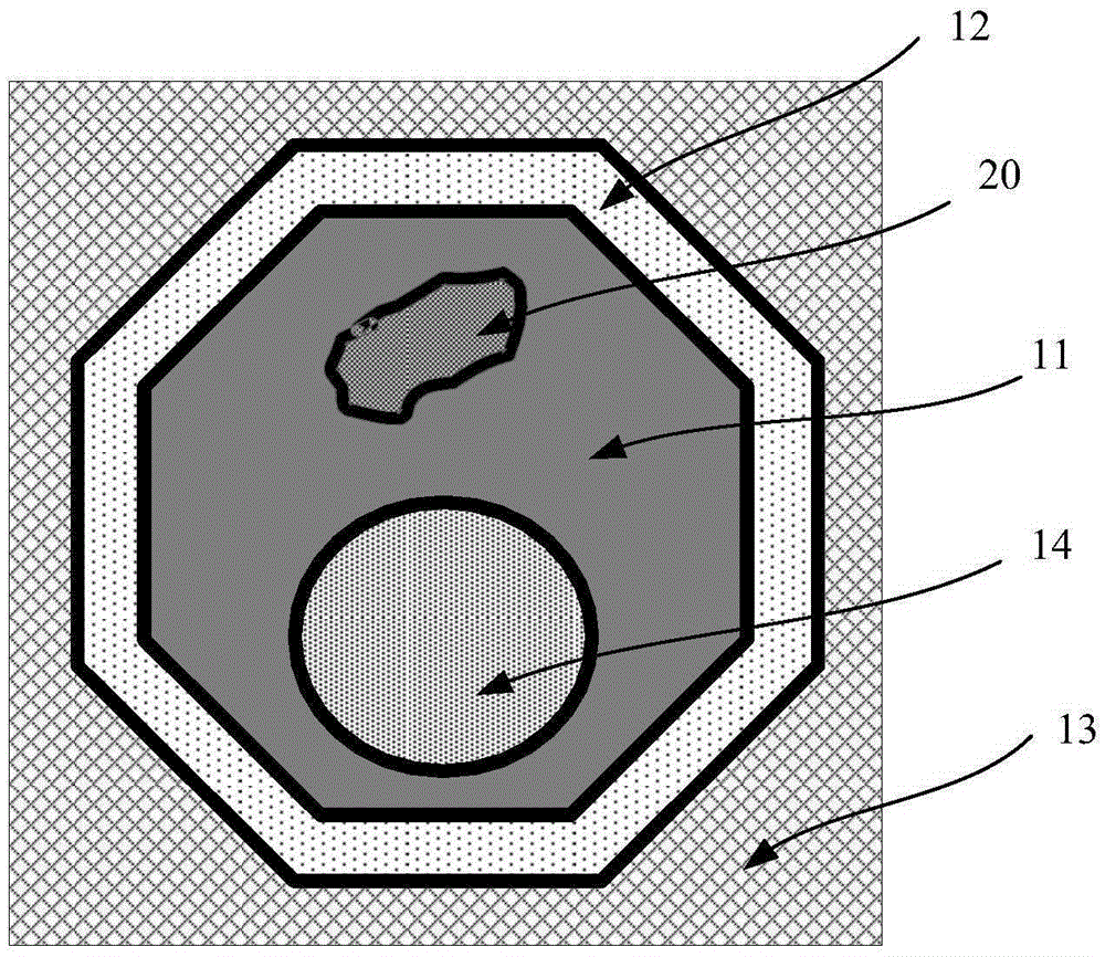
[0035] Such as Figure 4A As shown, a semiconductor wafer 10 is provided on which pads 11 and a first passivation layer 12 covering the semiconductor wafer 10 and exposing ...

Embodiment 2

[0058] Another embodiment of the present invention provides a semiconductor device, which can be prepared by the above-mentioned method.

[0059] Such as Figure 6 As shown, the semiconductor device 100 of this embodiment includes a semiconductor element 101 with a functional circuit and a packaging substrate 103, and the semiconductor element 101 and the packaging substrate 103 are connected by bumps 102 formed on the semiconductor element 101, wherein the The bump 102 is formed by the wafer bump manufacturing method provided by the present invention.

[0060] Wherein, the semiconductor element 101 may be an integrated circuit device for implementing various functions, such as various processor chips such as microprocessors and DSPs, or audio and video decoding chips, and the like.

[0061] The semiconductor device of this embodiment has high packaging reliability.

Embodiment 3

[0063] Still another embodiment of the present invention provides an electronic device, including a semiconductor device and an electronic component connected to the semiconductor device. Wherein, the semiconductor device is the above-mentioned semiconductor device.

[0064] Wherein, the electronic component may be any electronic component such as a discrete device or an integrated circuit.

[0065] The electronic device of this embodiment can be any electronic product or equipment such as mobile phone, tablet computer, notebook computer, netbook, game console, TV set, VCD, DVD, navigator, camera, video recorder, voice recorder, MP3, MP4, PSP, etc. , can also be any intermediate product including the semiconductor device.


PUM


Abstract

The invention provides a semiconductor wafer test method, and a wafer projection manufacturing method, a semiconductor device and an electronic device and relates to the technical field of a semiconductor. The semiconductor wafer test method comprises a step that during a probe test, test probe mark is made to deviate from the center position of a welding pad. The wafer projection manufacturing method comprises steps that during the probe test, the test probe mark is made to deviate from the center position of the welding pad, is utilized at a welding pad opening forming a wafer projection and is arranged at a region not influenced by the test probe mark. The semiconductor wafer test method and the wafer projection manufacturing method are advantaged in that influence of the test probe mark on manufacturing a ball bottom metal layer in the projection process can be completely prevented, a defect of projection missing can be avoided, packaging reliability is improved, and the packaging yield is further improved. The semiconductor device and the electronic device employing the semiconductor wafer test method and the wafer projection manufacturing method have similar advantages.

Description

technical field [0001] The present invention relates to the field of semiconductor technology, in particular to a semiconductor wafer testing method, a wafer bump manufacturing method, a semiconductor device formed by using the semiconductor wafer testing and bump manufacturing method, and a semiconductor device having the semiconductor device electronic device. Background technique [0002] With the development of portable and high-performance microelectronic products in the direction of shortness, smallness, lightness, and thinning, the traditional wire bonding method (Wire Bonding) as a packaging technology for combining chips with various substrates can no longer meet the needs of current consumer electronics products. Demand, replaced by bump packaging has become the key technology of wafer-level packaging. However, the manufacturing process of high-end chips is very complicated and the yield rate is difficult to control, while the yield rate of the bump manufacturing ...

Claims


Application Information

Patent Timeline
Patent Type & Authority Applications(China)
IPC IPC(8): H01L21/66H01L21/48
CPCH01L24/11H01L21/4814H01L22/14H01L2224/11
Inventor 金晨何文文杨莉娟
Owner SEMICON MFG INT (SHANGHAI) CORP
Why Eureka
Try Eureka