Display module packaging structure and preparation method thereof

A display module and packaging structure technology, applied in semiconductor/solid-state device manufacturing, semiconductor devices, electrical components, etc., can solve the problems of display devices not working properly, display module 12 damage, display module 12 erosion, etc., to achieve Inhibit the diffusion effect of the coating, improve the packaging effect, and inhibit the film layer from falling off

Active Publication Date: 2017-06-13
EVERDISPLAY OPTRONICS (SHANGHAI) CO LTD
View PDF5 Cites 18 Cited by
  • Summary
  • Abstract
  • Description
  • Claims
  • Application Information

AI Technical Summary

Problems solved by technology

[0004] However, due to the characteristics of the glass glue 13 itself and defects such as gaps between the cover glass 14 and the array substrate 11, the figure 1 The mechanical strength of the packaging structure shown in is weak, and it is easy to be damaged when encountering external impact, especially in the service life test, the above-mentioned p

Method used


Image

  • Display module packaging structure and preparation method thereof
  • Display module packaging structure and preparation method thereof
  • Display module packaging structure and preparation method thereof

Examples


Embodiment 1

[0074] Figure 2-7 It is a schematic flow diagram of preparing a display module packaging structure in the embodiment of the present application; as Figure 2-5 As shown, the present application provides a method for preparing a display module packaging structure, which may include the following steps:

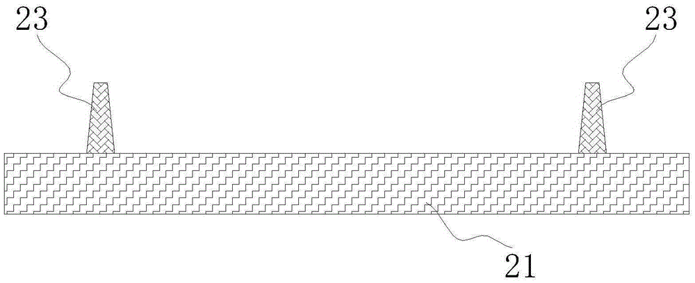
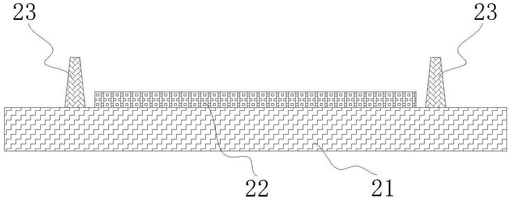
[0075] First, if figure 1 As shown, based on a base substrate (such as a low temperature polysilicon (LowTemperature PolySilicon, LTPS) substrate), the display device array (array) process is performed to form the array substrate 21; the above-mentioned array substrate 21 can be provided with In the display area and the non-display area set adjacent to the display area, the array substrate 21 in the display area is mainly used for attaching and preparing display devices; at the same time, thin film transistors can also be arranged on or in the array substrate 21 The display circuit is used to drive the subsequent display module to work.

[0076] In addition, during the abov...

Embodiment 2

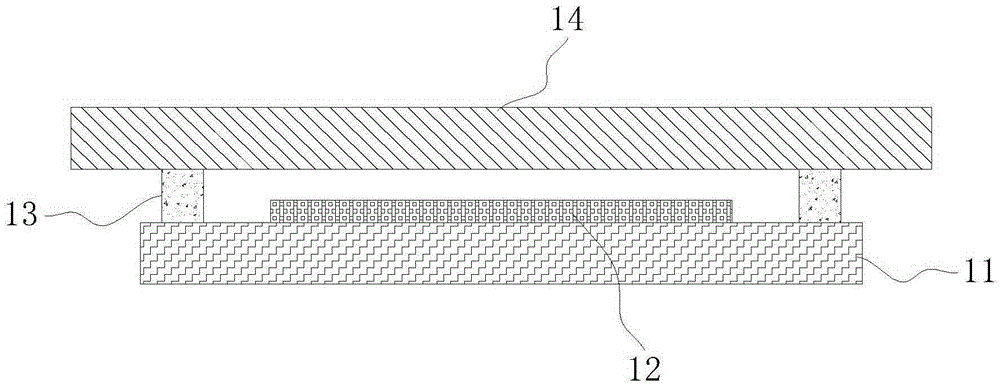
[0096] Can be based on the basis of the first embodiment above, such as Figure 7 As shown, the embodiment of the present application also provides a display module packaging structure, and the display module packaging structure can be used to prepare various display devices (such as OLED display devices, etc.), the above-mentioned display module packaging structure includes:

[0097] The array substrate 21 can be a substrate for completing the array (array) process, and can include but not limited to an LTPS substrate, etc.; the array substrate 21 can have a front surface for setting devices (i.e. Figure 5 shown in the upper surface) and the lower surface relative to the upper surface (ie Figure 5 , 6 The lower surface shown in ); the material of the substrate can be selected as glass, and the array substrate 21 can also be formed with a hard substrate or a flexible substrate, and the array substrate 21 can be provided with a device for driving a display module. Light-emi...


PUM

PropertyMeasurementUnit
Thicknessaaaaaaaaaa
Thicknessaaaaaaaaaa

Abstract

The invention provides a display module packaging structure and a preparation method thereof, and relates to the technical field of display devices. The display module packaging structure can be used for preparing related display devices such as AMOLEDs, a display module is sealed and protected by using a film packaging structure mainly, namely the display module is sealed by using a transparent inorganic film layer with a water and oxygen blocking characteristic, and inner stress and outer stress of the layer are buffered through the organic module prepared outside the inorganic film layer, and the film can be prevented from falling due to bending stress when the structure is used for manufacturing flexible devices. Meanwhile, a bulge structure formed by multi-layer stacking can effectively inhibit an inorganic layer coating film diffusion effect, the quantity of water-blocking baffle walls on the side face of the film device is increased, and the packaging effect can be effectively improved. Moreover, a role of supporting a metal mask is achieved in the film coating technology, and baseplate surface patterns are prevented from being damaged. Furthermore, film packaging is used for replacing a glass Frit glue packaging technology, so that the mechanical strength of the whole display device is effectively improved.

Description

technical field [0001] The invention relates to the technical field of display devices, in particular to a packaging structure of a display module and a preparation method thereof. Background technique [0002] In the display devices of electronic equipment, display electronic devices such as electrodeless light-emitting diodes (LEDs) or organic light-emitting diodes (OLEDs) used to generate light sources are key devices for the normal operation of display devices, but the above-mentioned electronic devices are extremely vulnerable The corrosion of moisture and oxygen in the external environment, so in order to ensure the normal operation of electronic devices, it is necessary to isolate and protect the display electronic devices. [0003] At present, glass glue (Frit) is mainly used to fix the cover glass on the array substrate, so as to seal the display electronic devices arranged on the array substrate; figure 1 As shown, in the traditional packaging structure of display...

Claims


Application Information

Patent Timeline
IPC IPC(8): H01L51/52H01L51/54H01L27/32
CPCH10K85/00H10K59/12H10K50/84H10K50/844
Inventor 何信儒吴建霖江欢
Owner EVERDISPLAY OPTRONICS (SHANGHAI) CO LTD
Why Eureka
Try Eureka