Check patentability & draft patents in minutes with Patsnap Eureka AI!

Method for forming fin field-effect transistor

A fin-type field effect and transistor technology, which is applied in semiconductor devices, semiconductor/solid-state device manufacturing, electrical components, etc., can solve the problems of transistor performance to be improved, and achieve the effect of improving interface performance, improving stability, and thin thickness

Active Publication Date: 2017-06-16
SEMICON MFG INT (SHANGHAI) CORP +1
View PDF3 Cites 2 Cited by
  • Summary
  • Abstract
  • Description
  • Claims
  • Application Information

AI Technical Summary

Problems solved by technology

[0007] The performance of the existing fin field effect transistors still needs to be improved

Method used


Image

  • Method for forming fin field-effect transistor
  • Method for forming fin field-effect transistor
  • Method for forming fin field-effect transistor

Examples


Embodiment Construction

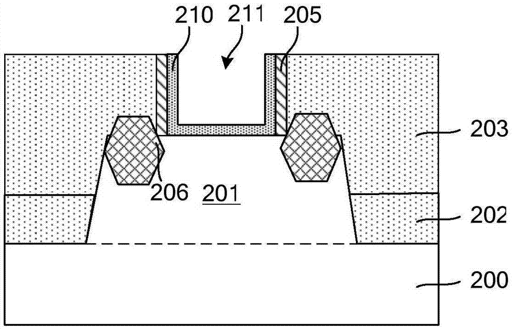
[0027] As mentioned in the background art, the performance of the existing fin field effect transistor still needs to be improved. To improve interface performance, it is necessary to form an interface layer on the surface of the fin before forming the high-K gate dielectric layer.

[0028] The study found that the existing interface layer is generally formed by oxidation process or deposition, and the material of the interface layer is GeO 2 , but GeO formed by prior art 2 The interface layer is very unstable and easily soluble in water, especially when exposed to air, it is easy to react with water vapor in the air; and because of the special structure of the fins, it is difficult to control the thickness of the interface layer, and the uniformity of the thickness It is also difficult to guarantee, and it is difficult to form a thinner thickness of GeO 2 interface layer.

[0029] Therefore, the present invention provides a method for forming a fin field effect transistor....


PUM

PropertyMeasurementUnit
thicknessaaaaaaaaaa
thicknessaaaaaaaaaa

Abstract

The invention relates to a method for forming a fin field-effect transistor, which comprises the steps of providing a semiconductor substrate, wherein the semiconductor substrate is provided with a fin portion, and the material of fin portion is Ge, SiGe or a III-V element; forming a pseudo grid which stretches across the side wall and the top surface of part of the fin portion; forming a dielectric layer covering the semiconductor substrate, the fin portion and the pseudo grid, wherein the surface of the dielectric layer is flush with the top surface of the pseudo grid; removing the pseudo grid, and forming a groove; forming a high-K dielectric layer containing oxygen ions at the side wall and the bottom surface of the groove; performing annealing on the high-K dielectric layer containing oxygen ions so as to enable the oxygen ions in the high-K dielectric layer containing oxygen ions to diffuse to the fin portion at the bottom of the groove, wherein the oxygen ions and the material of the fin portion react to form an interface layer; and forming a metal gate filling the groove on the high-K dielectric layer after annealing. Interface characteristics between the high-K dielectric layer and the fin portion of the fin field-effect transistor are improved according to the method.

Description

technical field [0001] The invention relates to the field of semiconductor manufacturing, in particular to a method for forming a fin field effect transistor. Background technique [0002] In the present invention, with the continuous development of semiconductor process technology, the process node is gradually reduced, and the gate-last process is widely used to obtain an ideal threshold voltage and improve device performance. However, when the feature size (CD, Critical Dimension) of the device is further reduced, even if the gate-last process is adopted, the structure of the conventional MOS field effect transistor can no longer meet the requirements for device performance, and the fin field effect transistor (Fin FET) as Substitution of conventional devices has received extensive attention. [0003] A fin field effect transistor in the prior art includes: a semiconductor substrate on which protruding fins are formed, and the fins are generally obtained by etching the s...

Claims


Application Information

Patent Timeline
Patent Type & Authority Applications(China)
IPC IPC(8): H01L21/336H01L21/324
CPCH01L29/66795H01L21/0228H01L21/02323H01L21/324
Inventor 谢欣云
Owner SEMICON MFG INT (SHANGHAI) CORP
Features
  • R&D
  • Intellectual Property
  • Life Sciences
  • Materials
  • Tech Scout
  • Unparalleled Data Quality
  • Higher Quality Content
  • 60% Fewer Hallucinations
Learn More