Terminal structure of FRD (Fast Recovery Diode) chip, preparation method thereof and FRD chip provided with terminal structure

A terminal structure and terminal technology, applied in semiconductor/solid-state device manufacturing, electrical components, circuits, etc., to achieve the effect of reducing production cost and area

Active Publication Date: 2017-06-16
EDGELESS SEMICON CO LTD OF ZHUHAI +1
View PDF6 Cites 0 Cited by
  • Summary
  • Abstract
  • Description
  • Claims
  • Application Information

AI Technical Summary

Problems solved by technology

[0003] The main purpose of the present invention is to provide a terminal structure of FRD chip, its preparation method and FRD chip with it, so as to solve the problem of how to improve the conductivity of the chip while ensuring the withstand voltage performance of the device

Method used


Image

  • Terminal structure of FRD (Fast Recovery Diode) chip, preparation method thereof and FRD chip provided with terminal structure
  • Terminal structure of FRD (Fast Recovery Diode) chip, preparation method thereof and FRD chip provided with terminal structure
  • Terminal structure of FRD (Fast Recovery Diode) chip, preparation method thereof and FRD chip provided with terminal structure

Examples


Embodiment Construction

[0029] It should be noted that, in the case of no conflict, the embodiments in the present application and the features in the embodiments can be combined with each other. The present invention will be described in detail below with reference to the accompanying drawings and examples.

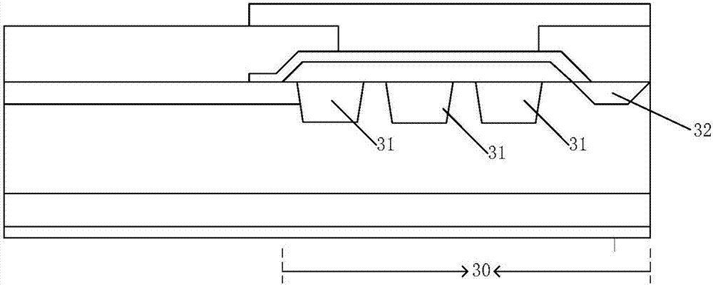
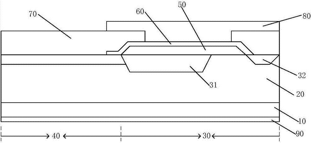
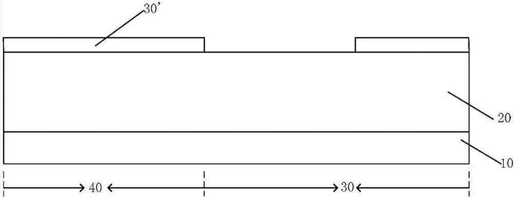
[0030] As mentioned in the background technology, the terminal area voltage is only to increase the breakdown voltage of the fast recovery diode, and has no contribution to the conductivity. Therefore, how to optimize the terminal withstand voltage structure and reduce the structural area of ​​​​the terminal area will help to improve the fast recovery diode. Conductivity, but reducing the area of ​​the terminal structure may lead to a decrease in the withstand voltage performance of the chip.

[0031] In order to solve the problem of how to improve the conductivity of the chip while ensuring the withstand voltage performance of the device, the inventors of the present application have found thr...


PUM


Abstract

The invention provides a terminal structure of an FRD (Fast Recovery Diode) chip, a preparation method thereof and an FRD chip provided with the terminal structure. The FRD chip is provided with a substrate and an epitaxial wafer arranged on the substrate. The FRD chip comprises the terminal structure and an active structure, wherein the terminal structure is arranged in the epitaxial wafer around the active structure of the FRD chip, and the extending direction of the substrate towards the epitaxial wafer is the depth direction. The terminal structure comprises a terminal voltage withstanding ring, a terminal stop ring, wherein the terminal voltage withstanding ring is arranged in the epitaxial wafer; the terminal stop ring is arranged in the epitaxial wafer at the side, which is away from the active structure, of the terminal withstanding ring, the substrate, the epitaxial wafer and the terminal stop ring are identical in the type of doping ions, and the doping ions of the terminal withstanding ring and doping ions of the epitaxial wafer are inversion ions. The number of the voltage withstanding ring is set to be one, so that the terminal structure is enabled to be greatly reduced in occupied area compared with the scheme of a voltage dividing ring in the prior art, and the terminal voltage withstanding ring has enough voltage withstanding performance. Therefore, the conductive capacity of the chip is improved, and the cost of manufacturing the terminal voltage withstanding ring is reduced.

Description

technical field [0001] The invention relates to the field of FRD chips, in particular to a terminal structure of an FRD chip, a preparation method thereof and an FRD chip having the same. Background technique [0002] Fast recovery diode (FRD) has the advantages of good switching performance, short reverse recovery time, and large forward current. It is often used in parallel with three-terminal power switching devices in power electronic circuits as a high-frequency, high-current freewheeling diode or rectifier At present, it has been widely used in induction cooker, power supply, frequency conversion household appliances, frequency conversion welding machine, electric vehicle and other products. According to the characteristics of the fast recovery diode, it is mainly used in the high-voltage field, so it is usually necessary to adopt terminal protection technology at the chip boundary of the fast recovery diode, that is, to set the terminal area to reduce the surface elec...

Claims


Application Information

Patent Timeline
Patent Type & Authority Applications(China)
IPC IPC(8): H01L29/06H01L21/329H01L29/861
CPCH01L29/0684H01L29/6609H01L29/861
Inventor 何昌肖婷包海涛
Owner EDGELESS SEMICON CO LTD OF ZHUHAI
Why Eureka
Try Eureka