LDMOS device and manufacturing method thereof

A device manufacturing method and device technology, applied in semiconductor/solid-state device manufacturing, semiconductor devices, electrical components, etc., can solve problems such as large impact of process fluctuations, and achieve the goals of avoiding process fluctuations, low on-resistance, and improving withstand voltage Effect

Inactive Publication Date: 2019-05-03
SHANGHAI HUALI MICROELECTRONICS CORP
View PDF5 Cites 0 Cited by
  • Summary
  • Abstract
  • Description
  • Claims
  • Application Information

AI Technical Summary

Problems solved by technology

However, this device has two disadvantages. One is that the drain 300 is no longer self-aligned implantation, which is greatly affected by process fluctuations; Reduce the voltage reaching under the gate 400 to avoid breakdown failure

Method used


Image

  • LDMOS device and manufacturing method thereof
  • LDMOS device and manufacturing method thereof
  • LDMOS device and manufacturing method thereof

Examples


Embodiment 1

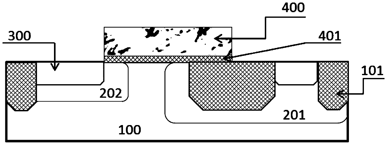
[0061] Such as Figure 4 As shown, the LDMOS device includes a first type well 206 formed on a silicon substrate 100;

[0062] A second type surface drift region 301, a drain terminal and a source terminal 300 are formed laterally of the first type well 206;

[0063] The surface drift region 301 is between the drain end and the source end 300, the surface drift region 301 is adjacent to the drain end, and is separated from the source end 300;

[0064] A silicon dioxide layer is formed above the surface drift region 301, and a silicon dioxide layer is formed above the interval between the homologous ends of the surface drift region 301;

[0065] The silicon dioxide layer directly above the surface drift region 301 is covered with an ONO film layer 402;

[0066] A polysilicon gate 400 is formed on the silicon dioxide layer above the interval between the ONO film layer 402 and the homologous end of the N-type surface drift region 301 .

[0067] Preferably, the depth of the sur...

Embodiment 2

[0074] The manufacturing method of the LDMOS device of embodiment one, comprises the following steps:

[0075] 1. Forming a pad silicon dioxide layer 403 on the silicon substrate 100;

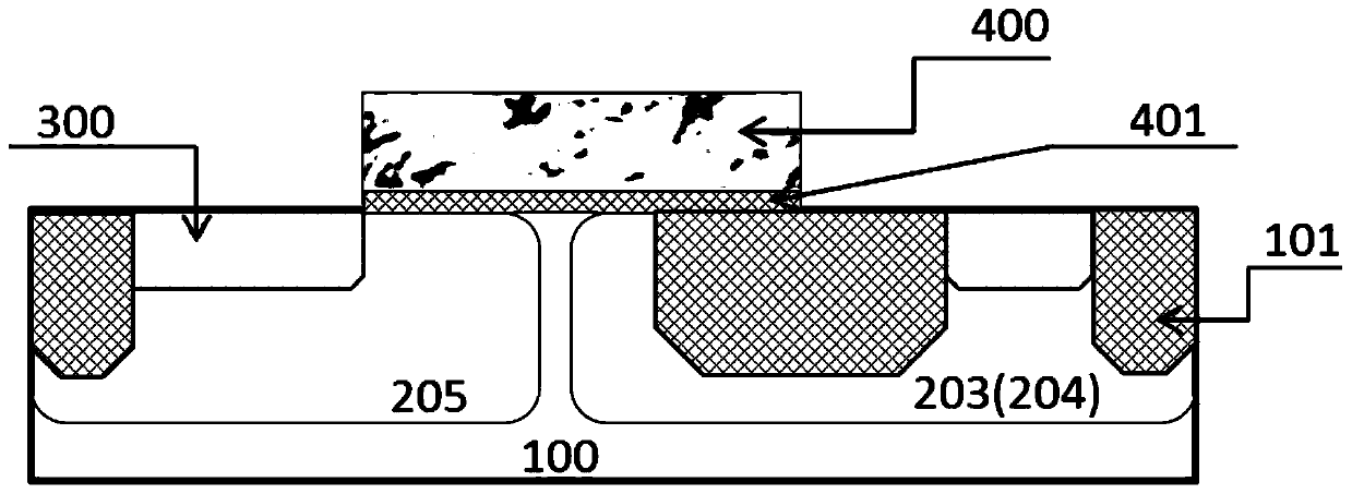
[0076] 2. On the silicon substrate 100, a shallow trench isolation region 101 is formed, such as Figure 5 shown;

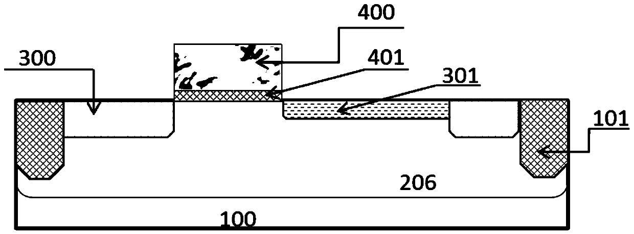
[0077] 3. On the right part of the silicon substrate 100 adjacent to the two shallow trench isolation regions 101, the surface drift region 301 is formed by photolithography and ion implantation through the pad silicon dioxide layer 403, and the surface drift region 301 shallower than the shallow trench isolation region 101, such as Figure 6 shown;

[0078] 4. Forming a first type well 206 on the entire upper part of the silicon substrate between two adjacent shallow trench isolation regions 101, the depth of the first type well 206 is not less than the depth of the shallow trench isolation region 101;

[0079] Five. Form ONO (silicon dioxide / silicon nitride / silicon dioxide) ...


PUM


Abstract

The invention discloses an LDMOS device. The LDMOS device comprises a well of a first type formed on a silicon substrate. A surface drift region of a second type, a drain end and a source end are formed in the transverse direction of the well of the first type. The surface drift region is arranged between drain end and the source end, is adjacent to the drain end, and is separated from the sourceend. A silicon dioxide layer is formed above the surface drift region, and a silicon dioxide layer is formed above a gap between the surface drift region and the source end. The silicon dioxide layerright above the surface drift region is covered by an ONO film layer, and a polysilicon gate is formed on the silicon dioxide layer above the gap between the ONO film layer and the gap between the N-type surface drift region and the source end. The invention also discloses a manufacturing method of the LDMOS device. According to the invention, the problem of device failure or reliability caused byprocess fluctuation can be avoided, and the process is controllable and has a small layout area under the premise of meeting high withstand voltage and low on-resistance.

Description

technical field [0001] The invention relates to semiconductor technology, in particular to an LDMOS device and a manufacturing method thereof. Background technique [0002] Lateral double-diffused metal oxide semiconductor (LDMOS) is a lightly doped MOS device, which has very good compatibility with CMOS technology. Traditional CMOS devices usually have a symmetrical source-drain structure, while LDMOS uses an asymmetric source-drain structure to meet the needs of higher withstand voltage and relatively low on-resistance. [0003] Such as figure 1 As shown, the source 300 region of the LDMOS is provided with a body region 202 , and the drain 300 region is provided with a drift region 201 . Wherein, the body region 202 is similar to the well region in a traditional CMOS transistor, and is mainly used to control the threshold voltage of the LDMOS; the drift region 201 is mainly used to control the withstand voltage performance of the LDMOS, and in order to improve the withst...

Claims


Application Information

Patent Timeline
Patent Type & Authority Applications(China)
IPC IPC(8): H01L29/06H01L29/40H01L29/78H01L21/336H01L21/265
Inventor 张强黄冠群
Owner SHANGHAI HUALI MICROELECTRONICS CORP
Why Eureka
Try Eureka