Plasma jet device

A plasma and jet device technology, applied in the field of plasma jet devices, can solve the problems of uneven plasma, uneven dry etching on the surface of the substrate, etc., and achieve the effects of high plasma particle activity and fast processing speed

Inactive Publication Date: 2017-06-16
BOE TECH GRP CO LTD +1
View PDF18 Cites 8 Cited by
  • Summary
  • Abstract
  • Description
  • Claims
  • Application Information

AI Technical Summary

Problems solved by technology

[0003] In order to solve the above problems, the present invention provides a plasma jet device, which at least partly solves t

Method used


Image

  • Plasma jet device
  • Plasma jet device
  • Plasma jet device

Examples


Embodiment 1

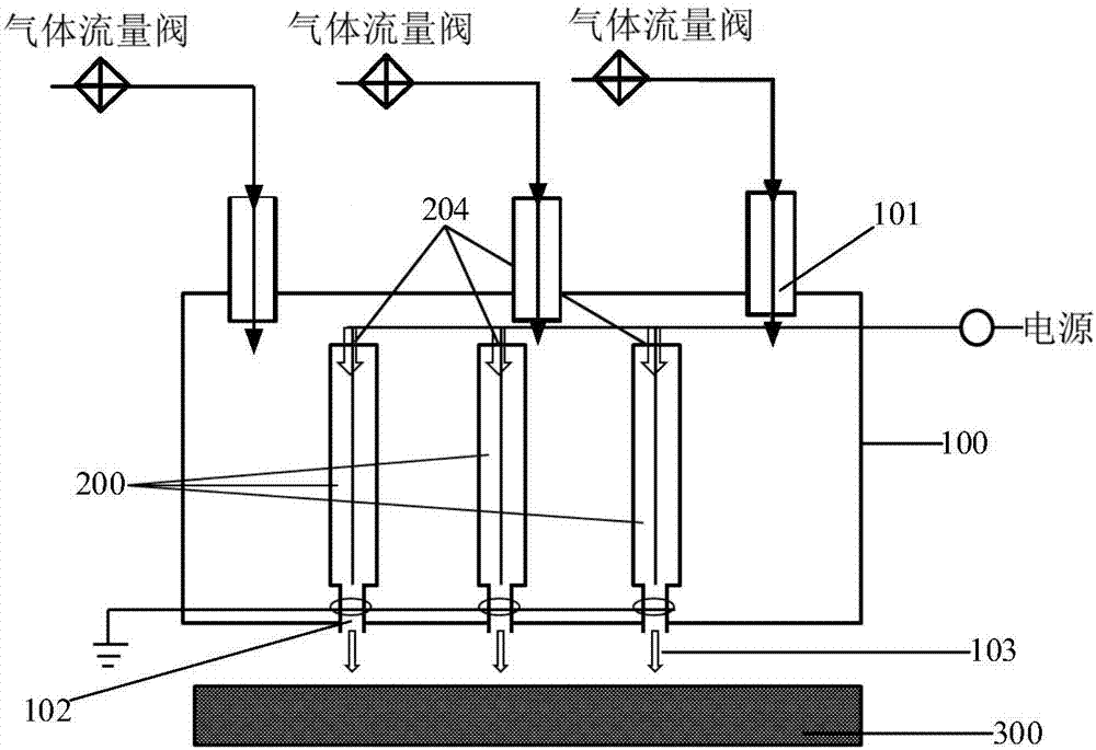
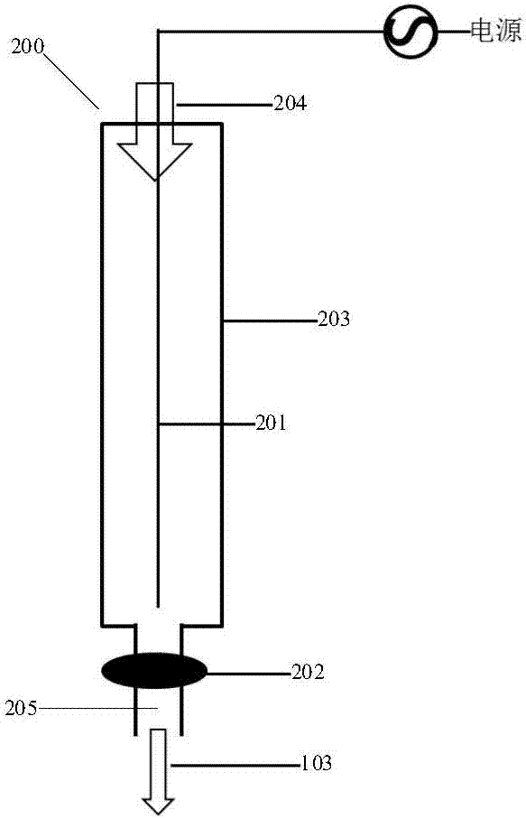
[0027] figure 1 It is a schematic structural diagram of a plasma jet device provided in Embodiment 1 of the present invention. Such as figure 1 As shown, the plasma jet device includes a housing 100 surrounding and forming a discharge space. The housing 100 is provided with a first inlet 101 and a first outlet 102 , and a plurality of discharge units 200 are distributed in the housing 100 . The first inlet 101 is used to supply the reactive gas to the discharge unit 200, the discharge unit 200 is used to discharge the reactive gas to form a plasma jet 103, and the first outlet 102 is used to output The plasma jet 103 . The plasma formed by the plasma jet device provided in this embodiment forms large-area uniform and stable plasma jets 103 through the action of air flow, and these arrayed plasma jets 103 directly act on the substrate 300 to etch the thin film transistor, and finally A thin film transistor plasma etching process that separates the discharge area from the wo...

Embodiment 2

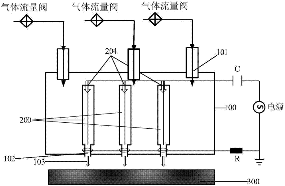
[0033] image 3 It is a schematic structural diagram of a plasma jet device provided in Embodiment 2 of the present invention. Such as image 3 As shown, the plasma jet device includes a housing 100 on which a first inlet 101 and a first outlet 102 are disposed, and a plurality of discharge units 200 are distributed in the housing 100 . The first inlet 101 is used to supply the reactive gas to the discharge unit 200, the discharge unit 200 is used to discharge the reactive gas to form a plasma jet 103, and the first outlet 102 is used to output The plasma jet 103 . The plasma formed by the plasma jet device provided in this embodiment forms large-area uniform and stable plasma jets 103 through the action of air flow, and these arrayed plasma jets 103 directly act on the substrate 300 to etch the thin film transistor, and finally A thin film transistor plasma etching process that separates the discharge area from the work area. The technical solution provided in this embodi...

Embodiment 3

[0040] Figure 5 It is a schematic structural diagram of a plasma jet device provided in Embodiment 3 of the present invention. It should be noted that the difference between the plasma jet device provided in this embodiment and the plasma jet device provided in Embodiment 1 lies in the arrangement of the discharge cells 200, therefore Figure 5 Mainly shows the arrangement of the discharge unit 200, for other parts of the plasma jet device, please refer to figure 1 . see figure 1 with Figure 5 , the plasma jet device includes a casing 100, on which a first inlet 101 and a first outlet 102 are arranged, and a plurality of discharge units 200 are distributed in the casing 100. The first inlet 101 is used to supply the reactive gas to the discharge unit 200, the discharge unit 200 is used to discharge the reactive gas to form a plasma jet 103, and the first outlet 102 is used to output The plasma jet 103 . The plasma formed by the plasma jet device provided in this embodi...


PUM


Abstract

The invention discloses a plasma jet device comprising a shell which is provided with a first inlet and a first outlet. Multiple discharge units are distributed in the shell. The first inlet is used for providing reaction gas to the discharge units. The discharge units are used for performing discharge processing on the reaction gas so as to form plasma jet. The first outlet is used for outputting the plasma jet. According to the plasma jet device, the formed plasmas form a large area of uniform and stable plasma jet through the effect of gas flow, the array plasma jet directly affects a substrate to perform etching on a thin film transistor, and finally the thin film transistor plasma etching technology in which a discharge area and a working area are separated can be realized. The technical scheme has the advantages of being high in plasma particle activity and fast in processing speed so as to realize multi-angle and large area of uniform and stable low temperature thin film transistor surface etching.

Description

technical field [0001] The invention relates to the field of display technology, in particular to a plasma jet device. Background technique [0002] The existing plasma device pumps the process chamber to a high vacuum state through a vacuum pump, then opens the flow valve of the etching gas, fills the reaction gas into the process chamber, and finally connects the radio frequency power supply, and the etching gas generates plasma through glow discharge The above-mentioned plasma contains etching substances required for etching reactions such as electrons, ions, and active reactive groups. However, the plasma generated by the existing plasma device is not uniform, resulting in non-uniform dry etching on the surface of the substrate. Contents of the invention [0003] In order to solve the above problems, the present invention provides a plasma jet device, which at least partly solves the problem of non-uniform plasma generated by existing plasma devices, resulting in non-...

Claims


Application Information

Patent Timeline
IPC IPC(8): H05H1/24H01L21/336
CPCH01L29/66234H05H1/24
Inventor 占建英周如张俊张慧文元淼
Owner BOE TECH GRP CO LTD
Why Eureka
Try Eureka