
MEMS micro Raman spectrometer

A Raman spectrometer, a miniature technology, used in Raman scattering, material excitation analysis, etc., can solve the problems of unguaranteed, narrow full width at half maximum, high price, etc., to achieve reduced equipment size, high spectral resolution, and easy equipment. volume effect

Pending Publication Date: 2017-06-20
XUZHOU NORMAL UNIVERSITY
View PDF4 Cites 8 Cited by
  • Summary
  • Abstract
  • Description
  • Claims
  • Application Information

AI Technical Summary

Problems solved by technology

However, because the intensity of Raman scattering is very weak, and its intensity is 10-6 to 10-3 times that of Rayleigh scattering light, the structure of Raman spectrometers is generally complicated and expensive, often costing millions of RMB. It hinders the application of Raman spectroscopy in practical detection, and the miniaturization and simplification of Raman spectroscopy instruments will be the future development direction
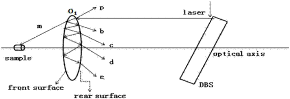
[0003] However, in order to ensure the compactness of the system, the micro-Raman spectrometer currently used for on-site emergency detection usually has the same optical path as the laser illumination system of the sample and the lens of the Raman scattered light, so that it is inevitable to generate a lot of light in the light-collecting lens. secondary reflection, forming stray light other than Rayleigh scattered light, but the detection of Raman spectroscopy belongs to weak signal detection, and the stray light in the system needs to be strictly suppressed. In addition, the existing portable Raman spectrometer generally uses a portable computer to complete data processing. Due to the inherent contradiction between the resolution and the focal length of the grating dispersion technology, the existing spectrometer cannot guarantee to obtain a narrow full width at half maximum while having a wide free spectral range.

Method used


Image

  • MEMS micro Raman spectrometer
  • MEMS micro Raman spectrometer
  • MEMS micro Raman spectrometer

Examples


Embodiment 1

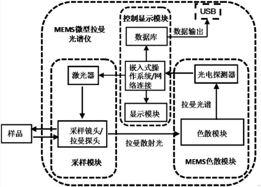
[0028] Embodiment 1: as figure 1 As shown, the present embodiment provides a MEMS miniature Raman spectrometer, including a sampling module, a control display module, and a MEMS dispersion module;

[0029] The sampling module includes a laser, a sampling lens / Raman probe system;

[0030] The control display module includes a database unit, an embedded operating system / network connection unit, and a display module;

[0031] The MEMS dispersion module includes a dispersion module and a photodetector unit;

[0032] The light emitted by the laser passes through the sampling lens / Raman probe system, and is irradiated on the sample to excite the Raman spectrum. Afterwards, it is transmitted to the photodetector unit to obtain a new Raman spectrum. By comparing the new Raman spectrum with the data of the database unit, the identity information of the measured object is displayed on the display module;

[0033] The system control and data exchange and processing of the whole instru...


PUM

PropertyMeasurementUnit
Wavelengthaaaaaaaaaa
Bandwidthaaaaaaaaaa
Slit widthaaaaaaaaaa

Abstract

The invention discloses an MEMS micro Raman spectrometer, which includes a sampling module, a control display module, and an MEMS dispersion module. All the modules of the MEMS micro Raman spectrometer have higher integration degree, the equipment volume can be reduced more easily, and a handheld spectrometer can be made. Also the MEMS micro Raman spectrometer can strictly inhibit the stray light genegrated by a laser lighting system and a lens common optical path of Raman scattering light. The MEMS micro Raman spectrometer provided by the invention adopts an embedded operating system to complete data processing function, can realize handheld use, and can completely break away from computers to work independently. The MEMS micro Raman spectrometer provided by the invention adopts MEMS technology grating and movable F-P cavity integrated dispersion, can guarantee a wide free spectral range, at the same time can acquire narrow full width at half-maximum, and can acquire high spectral resolution.

Description

technical field [0001] The invention relates to the field of optical detection instruments, in particular to a MEMS miniature Raman spectrometer. Background technique [0002] The Raman spectrum reflects the vibration characteristics of atoms in the molecular structure, which is called the fingerprint spectrum of the molecule. As an unparalleled and powerful analysis method, Raman detection technology has the advantages of non-destructive measurement, fast detection speed, simple sample preparation, and on-site detection. It is expected to be applied in real production and life. However, because the intensity of Raman scattering is very weak, and its intensity is 10-6 to 10-3 times that of Rayleigh scattering light, the structure of Raman spectrometers is generally complicated and expensive, often costing millions of RMB. It hinders the application of Raman spectroscopy in practical detection, and the miniaturization and simplification of Raman spectroscopy instruments will...

Claims


Application Information

Patent Timeline
IPC IPC(8): G01N21/65
CPCG01N21/65
Inventor 聂新明田亚平韩彩芹朱超
Owner XUZHOU NORMAL UNIVERSITY
Learn More