Epitaxial method for improving the breakdown voltage of GaN-based power devices

A power device and breakdown voltage technology, which is applied in semiconductor/solid-state device manufacturing, circuits, electrical components, etc., can solve the problem that the high voltage resistance is not as good as the breakdown voltage value

Active Publication Date: 2019-08-06
SHANGHAI SIMGUI TECH
View PDF3 Cites 0 Cited by
  • Summary
  • Abstract
  • Description
  • Claims
  • Application Information

AI Technical Summary

Problems solved by technology

[0004] Although the theoretical breakdown voltage of GaN materials is very high, the high voltage withstand capability of current GaN power devices is far less than the theoretically calculated breakdown voltage.

Method used


Image

  • Epitaxial method for improving the breakdown voltage of GaN-based power devices
  • Epitaxial method for improving the breakdown voltage of GaN-based power devices
  • Epitaxial method for improving the breakdown voltage of GaN-based power devices

Examples


Embodiment Construction

[0017] The specific implementation of the epitaxial method for increasing the breakdown voltage of GaN-based power devices provided by the present invention will be described in detail below with reference to the accompanying drawings.

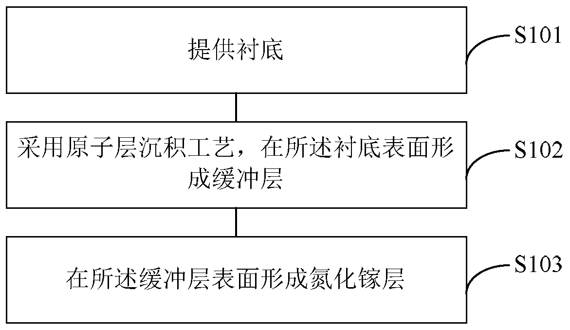
[0018] Please refer to figure 1 , is a schematic flow chart of an epitaxial method for increasing the breakdown voltage of GaN-based power devices according to a specific embodiment of the present invention.

[0019] The epitaxial method for increasing the breakdown voltage of GaN-based power devices includes the following steps:

[0020] Step S101: providing a substrate; Step S102: forming a buffer layer on the surface of the substrate by using an atomic layer deposition process; Step S103: forming a gallium nitride layer on the surface of the buffer layer.

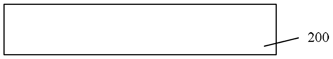
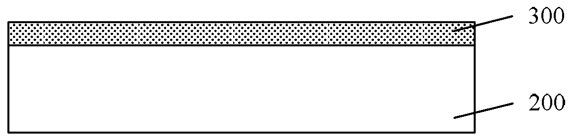
[0021] Please refer to Figure 2 to Figure 4 It is a schematic cross-sectional structure diagram of an epitaxial process for increasing the breakdown voltage of GaN-based power devices...


PUM


Abstract

The invention relates to an epitaxial method for improving a breakdown voltage of a GaN-based power device. The epitaxial method comprises the steps of providing a substrate; forming a buffer layer on a surface of the substrate by an atomic layer deposition process; and forming a GaN layer on a surface of the buffer layer. With the method, the quality of formed GaN can be improved.

Description

technical field [0001] The invention relates to the technical field of semiconductors, in particular to an epitaxy method for improving the breakdown voltage of gallium nitride-based power devices. Background technique [0002] Wide bandgap semiconductor materials represented by gallium nitride (GaN) have superior properties such as large bandgap, high breakdown electric field, high thermal conductivity, high electron saturation drift velocity, strong radiation resistance and good chemical stability. . It has unique advantages in the production of microwave high-power devices, high-temperature-resistant devices and radiation-resistant devices. GaN-based power devices are currently a cutting-edge hot technology that is vigorously developed internationally, and are also the core technology of key power electronics technologies that are urgently needed in my country's energy development. [0003] The wide bandgap semiconductor materials of group III nitrides represented by ga...

Claims


Application Information

Patent Timeline
Patent Type & Authority Patents(China)
IPC IPC(8): H01L21/205
CPCH01L21/2056
Inventor 闫发旺张峰赵倍吉刘春雪李晨
Owner SHANGHAI SIMGUI TECH
Why Eureka
Try Eureka