Preparation method of silicon nanosheet array

A technology for silicon nanosheets and arrays is applied in the field of preparation of silicon nanosheet arrays, which can solve the problems of low density and uncontrollable morphology, and achieve the effects of uniform size, reduction of dangling bonds and simple preparation method.

Active Publication Date: 2021-02-26
CHONGQING UNIV OF ARTS & SCI
View PDF2 Cites 0 Cited by
  • Summary
  • Abstract
  • Description
  • Claims
  • Application Information

AI Technical Summary

Problems solved by technology

This method is simple and efficient to prepare high-density and controllable nanosheet arrays, which solves the problems of low density and uncontrollable morphology in the current preparation of silicon nanosheet arrays.

Method used


Image

  • Preparation method of silicon nanosheet array
  • Preparation method of silicon nanosheet array
  • Preparation method of silicon nanosheet array

Examples


Embodiment 1

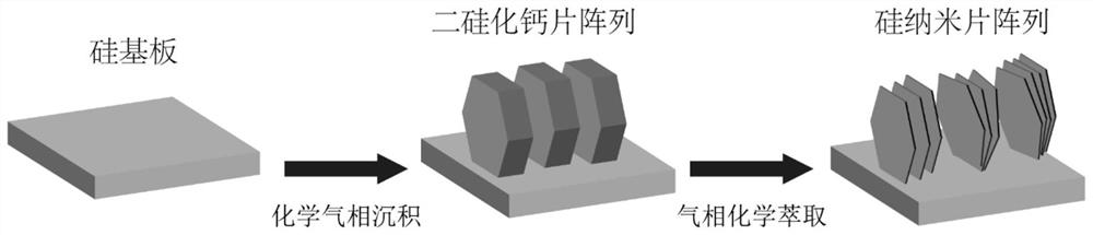
[0033] A method for preparing a silicon nanosheet array, carried out as follows:

[0034] (1) Silicon substrate pretreatment

[0035] Set the size to 8*8mm 2 , a thickness of about 1 mm, and a single crystal silicon substrate with a crystal plane of (111) was soaked in 50 mL of acetone solution for ultrasonication, and then evaporated to the remaining 15 mL of acetone solution. : Soak in the mixed solution formed by the volume ratio of 1:2 for 10 seconds, rinse with pure water, and finally dip it in an aqueous solution of hydrofluoric acid with a volume fraction of 8% for cleaning, and dry it in the air after washing;

[0036] (2) Preparation of silicide precursor

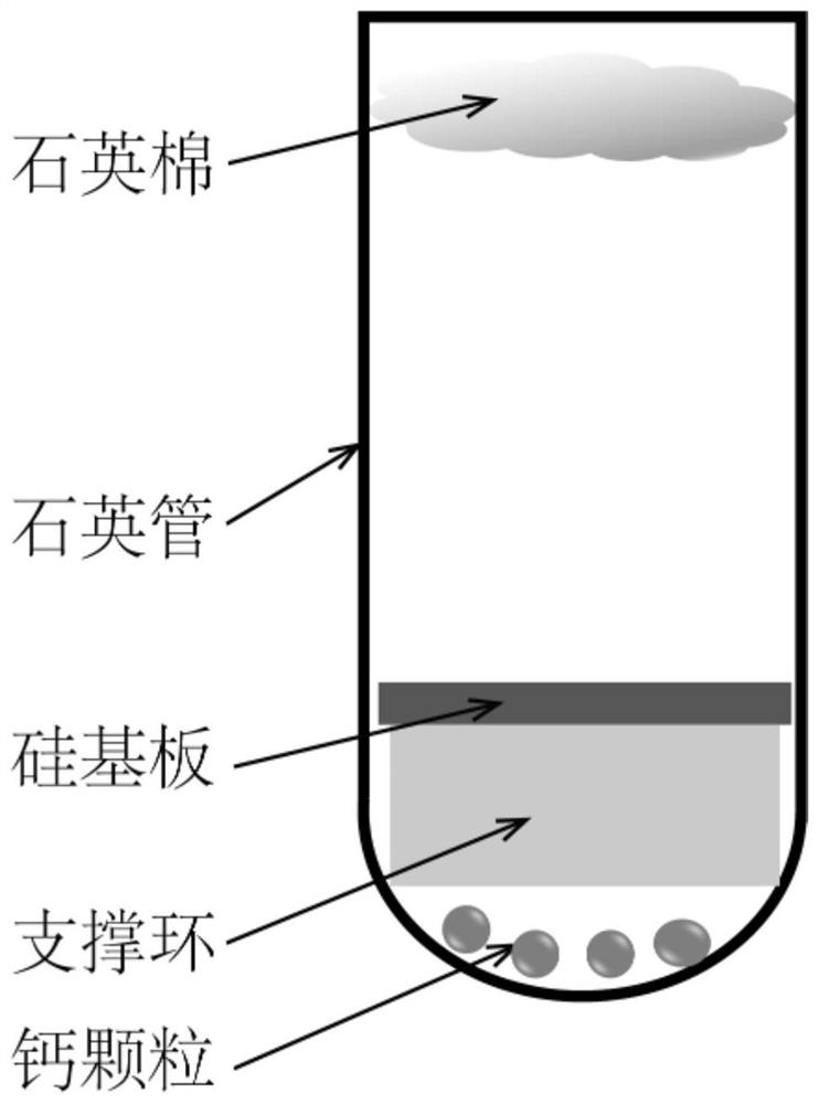
[0037] Place the pretreated silicon substrate and 0.025g of calcium metal particles in an adaptation container, the calcium metal particles are at the bottom of the quartz container, the silicon substrate is at the upper end of the calcium metal particles, and keep a certain distance, face down, and use the quart...

Embodiment 2

[0044] A method for preparing a silicon nanosheet array, carried out as follows:

[0045] (1) Silicon substrate pretreatment

[0046] Set the size to 8*8mm 2 , a thickness of about 1 mm, and a single crystal silicon substrate with a crystal plane of (111) was soaked in 50 mL of acetone solution for ultrasonication, and then evaporated to the remaining 15 mL of acetone solution. : Soak in the mixed solution formed by the volume ratio of 1:2 for 10 seconds, rinse with pure water, and finally dip it in a hydrofluoric acid aqueous solution with a volume fraction of 10%, and dry it in the air after washing;

[0047] (2) Preparation of silicide precursor

[0048] Place the silicon substrate and 0.03g of calcium metal particles in an adaptation container, the calcium metal particles are at the bottom of the quartz container, the silicon substrate is at the upper end of the calcium metal particles, and keep a certain distance, face down, and the quartz container mouth is sealed with...

Embodiment 3

[0055] A method for preparing a silicon nanosheet array, carried out as follows:

[0056] (1) Silicon substrate pretreatment

[0057] Set the size to 8*8mm 2 , a thickness of about 1 mm, and a single crystal silicon substrate with a crystal plane of (111) was soaked in 50 mL of acetone solution for ultrasonication, and then evaporated to the remaining 15 mL of acetone solution. : Soak in the mixed solution formed by the volume ratio of 1:2 for 10 seconds, rinse with pure water, and finally dip it with a hydrofluoric acid aqueous solution with a volume fraction of 5% for cleaning, and dry it in the air after washing;

[0058] (2) Preparation of silicide precursor

[0059] Place the silicon substrate and 0.02g of calcium metal particles in an adaptation container, the calcium metal particles are at the bottom of the quartz container, the silicon substrate is at the upper end of the calcium metal particles, and keep a certain distance, face down, and the quartz container mouth ...


PUM

PropertyMeasurementUnit
thicknessaaaaaaaaaa
thicknessaaaaaaaaaa
thicknessaaaaaaaaaa

Abstract

The invention relates to a preparation method of a silicon nanosheet array, which comprises the following steps: pretreating a silicon substrate with a crystal face (111), sequentially carrying out sectional heating reaction on the pretreated silicon substrate and calcium in vacuum at 630-640 DEG C and 700-720 DEG C, cooling a reaction product to room temperature after the reaction is completed, soaking the reacted silicon substrate in an ethanol solution of manganese chloride for 2 hours, and respectively putting the soaked silicon substrate and manganese chloride granules at two ends of a sectional heating furnace; by introducing nitrogen in the whole process, heating the end, in which the manganese chloride granules are arranged, to 700-830 DEG C, and heating the other end, in which thesubstrate is arranged, to 500-600 DEG C, thus carrying out heat preservation reaction; and cooling the reaction system to room temperature after the reaction is finished. The prepared silicon nanosheets are perpendicular to the silicon substrate and form an array, the distance between the nanosheets reaches 10-100 nm, the nanosheets are not agglomerated or collapsed, the thickness of the nanosheets can be effectively regulated and controlled within 5-150 nm, the height reaches about 2 microns, the yield is high and can reach 55.7-63.9% of that of raw materials, a high-density silicon nanosheet array is formed, and the purity reaches up to 96.4%.

Description

technical field [0001] The invention relates to the technical field of silicon nanometer materials, in particular to a method for preparing a silicon nanosheet array. Background technique [0002] Silicon is an abundant and environment-friendly element, and it is also the basic material of modern electronics industry and photovoltaic industry. At the same time, silicon is also used in new industries such as degradable electronic sensors, drug delivery devices, and lithium battery anode materials. Recently, the preparation methods of low-dimensional silicon nanomaterials have been greatly developed, such as chemical vapor deposition and chemical etching. At present, there are relatively few studies on two-dimensional silicon nanosheets, mainly due to the cubic structure of sp3 hybridization of silicon, which makes it difficult to self-assemble into two-dimensional nanostructure materials with atomic thickness, but silicon nanosheets show excellent electrical properties. , O...

Claims


Application Information

Patent Timeline
Patent Type & Authority Applications(China)
IPC IPC(8): C01B33/021B82Y40/00H01M10/052H01M4/38
CPCC01B33/021B82Y40/00H01M4/386H01M10/052Y02E60/10
Inventor 孟祥程江唐华李璐立冈浩一
Owner CHONGQING UNIV OF ARTS & SCI
Why Eureka
Try Eureka