Semiconductor packaging part and manufacturing method therefor

A semiconductor and packaging technology, applied in the field of semiconductor packaging to prevent warping and its manufacturing, can solve problems such as limited and limited thickness, and achieve the effects of improving durability, controlling warping, and solving unevenness

Inactive Publication Date: 2017-06-20
SAMSUNG SEMICON CHINA RES & DEV +1
View PDF8 Cites 1 Cited by
  • Summary
  • Abstract
  • Description
  • Claims
  • Application Information

AI Technical Summary

Problems solved by technology

[0005] However, although this design can reduce the warpage of the semiconductor package, because the thickness of the redistribution structure of the semiconductor package is limited, the ability to balance the warpage through the compressive stress layer arranged in the redistribution structure is limited, and it does not Enables precise control of warpage defects produced by epoxy molding compounds (EMC)

Method used


Image

  • Semiconductor packaging part and manufacturing method therefor
  • Semiconductor packaging part and manufacturing method therefor
  • Semiconductor packaging part and manufacturing method therefor

Examples


Embodiment Construction

[0029] Hereinafter, embodiments of the present invention will be described in detail with reference to the accompanying drawings. In the drawings, in order to clearly show main elements related to the inventive concept, the shapes of layers or regions may be exaggerated, and minor elements may be omitted to avoid ambiguity of expression. The inventive concept is not limited to the following embodiments, and the features, elements or structures involved in each embodiment or corresponding method descriptions can be applied to other embodiments individually or in combination.

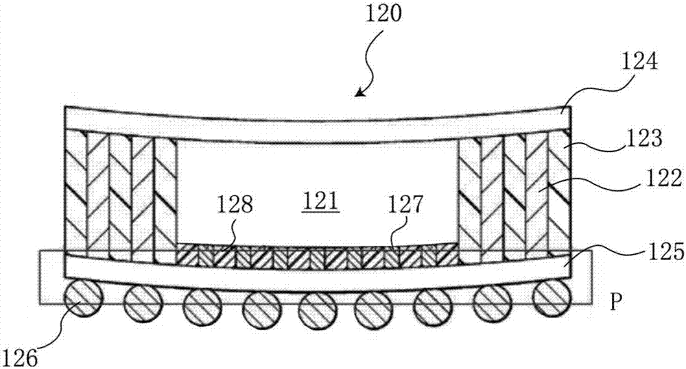
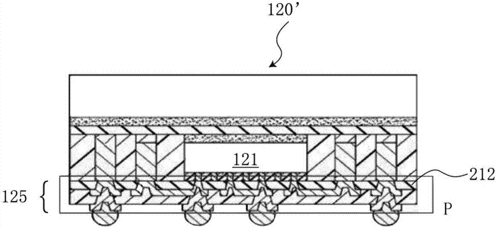
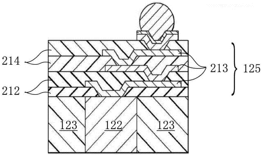
[0030] Figure 4 is a schematic diagram of a semiconductor package according to an embodiment of the present invention. Such as Figure 4 As shown, the semiconductor package 100 includes a substrate 110 , a dielectric layer 120 , a redistribution structure 130 , a semiconductor chip 140 and an encapsulation layer 150 . The substrate 110 is formed of molding material. In one embodiment, the substrate 1...


PUM


Abstract

The invention provides a semiconductor packaging part and a manufacturing method therefor. The semiconductor packaging part comprises a substrate, a dielectric layer, a rewiring structure, a semiconductor chip, and an encapsulating layer, wherein the substrate comprises a first surface, a second surface back to the first surface, and conductive columns which extend in the substrate to connect the first surface and the second surface; the dielectric layer is positioned on the first surface of the substrate; the rewiring structure is arranged in the dielectric layer and electrically connected to the conductive columns; the semiconductor chip is arranged on the dielectric layer and electrically connected to the rewiring structure; and the encapsulating layer is positioned on the dielectric layer and encapsulates the semiconductor chip, wherein each of the substrate and the encapsulating layer is formed by a moulding material.

Description

technical field [0001] The invention relates to the field of semiconductor packages, in particular to a semiconductor package for preventing warping and a manufacturing method thereof. Background technique [0002] With the rapid popularization of electronic products such as mobile phones, tablet computers, and digital cameras, semiconductor packages are being used more and more widely. Generally, a flip chip ball grid array (Flip-Chip Ball Grid Array, FCBGA) semiconductor package is a typical package structure. In the package structure, an active surface of at least one semiconductor chip may be electrically connected to one surface of the substrate via a plurality of conductive bumps. An underfill is filled between the semiconductor chip and the substrate so that the underfill of the semiconductor chip surrounds the conductive bumps and fills spaces between the conductive bumps to enhance the strength of the conductive bumps and support the semiconductor chip. Meanwhile,...

Claims


Application Information

Patent Timeline
Patent Type & Authority Applications(China)
IPC IPC(8): H01L23/498H01L23/29H01L23/31H01L21/56
CPCH01L21/56H01L23/293H01L23/3128H01L23/49894H01L2924/181H01L21/4857H01L23/49822H01L23/5389H01L23/49816H01L23/49827H01L2224/16238H01L24/16H01L2924/00014H01L2924/00012H01L2224/13099H01L23/485H01L23/28H01L24/12H01L24/11H01L23/49811H01L21/563H01L21/486H01L2224/12H01L24/19H01L2224/16225
Inventor 李轶楠
Owner SAMSUNG SEMICON CHINA RES & DEV
Why Eureka
Try Eureka