III-V CMOS type persudomorphic heterojunction field effect transistor

A heterojunction field effect and transistor technology, applied in the direction of transistors, electric solid-state devices, semiconductor devices, etc., can solve difficult problems such as reducing power consumption, avoiding lattice relaxation, and overcoming the difficulty of matching atomic lattices Effect

Active Publication Date: 2017-07-14
CHENGDU HIWAFER SEMICON CO LTD
View PDF5 Cites 5 Cited by
  • Summary
  • Abstract
  • Description
  • Claims
  • Application Information

AI Technical Summary

Problems solved by technology

[0006] The purpose of the present invention is to provide a III-V CMOS type pseudo-heterojunction field effect transistor, which can well solve the problem of difficulty in reducing power consumption and short channel effect of existing transistors in the process of scaling down. problem to overcome

Method used


Image

  • III-V CMOS type persudomorphic heterojunction field effect transistor

Examples


Embodiment Construction

[0018] In order to make the purpose, technical solution and advantages of the present application clearer, the present application will be further described in detail below in conjunction with the accompanying drawings and specific embodiments. For simplicity, some technical features known to those skilled in the art are omitted from the following description.

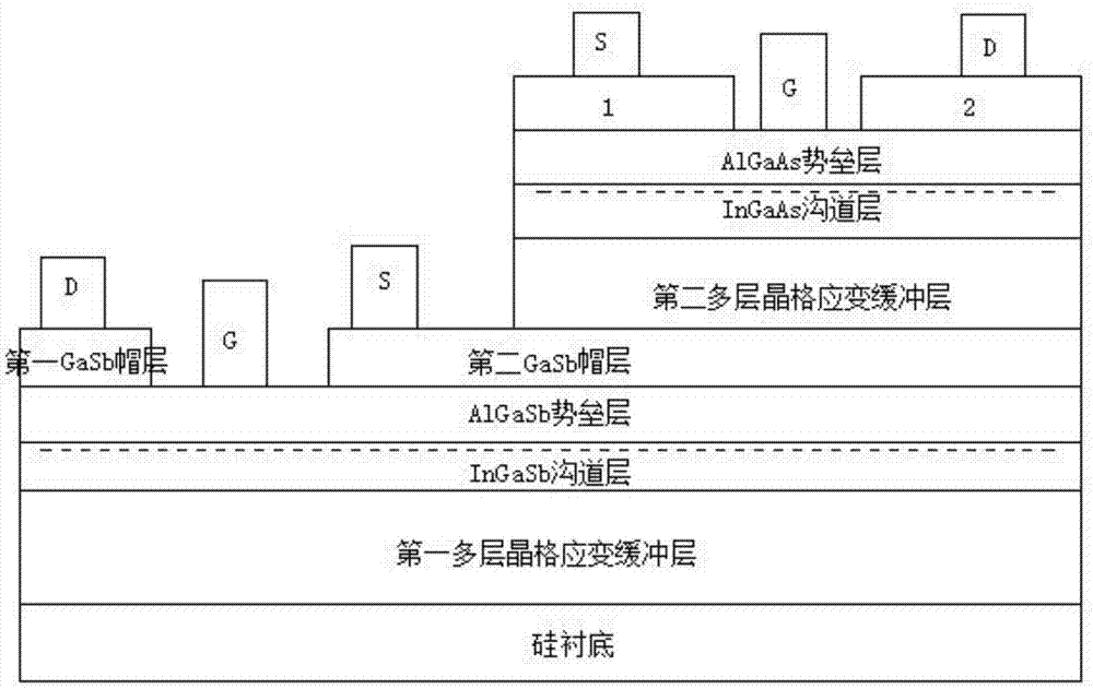
[0019] like figure 1 As shown, this embodiment provides a III-V CMOS type pseudo-heterojunction field effect transistor, which is epitaxially grown by MOCVD or MBE equipment, and includes a P-channel transistor and an n-channel transistor; the P-channel transistor is formed on a silicon substrate The first multi-layer lattice strain buffer layer, the InGaSb channel layer and the AlGaSb barrier layer are epitaxially grown in sequence, the first GaSb cap layer and the second GaSb cap layer are grown on the AlGaSb barrier layer, and the InGaSb channel layer and the AlGaSb A two-dimensional hole gas is formed in a region ...


PUM


Abstract

The invention relates to the technical field of semiconductor device production and specifically relates to a wide band gap III-V CMOS type persudomorphic heterojunction field effect transistor which is based on a silicon substrate and combines an n channel transistor and a p channel transistor. According to the heterojunction field effect transistor, a material is epitaxially grown through adoption of an MOCVD or MBE device. The heterojunction field effect transistor is composed of a first multilayer lattice strain buffer layer, an InGaSb channel layer, an AlGaSb barrier layer, a GaSb cap layer, a second multilayer lattice strain buffer layer, an InGaAs channel layer, an AlGaAs barrier layer and an In<X>Ga<1-X>As cap layer which are epitaxially grown on a high resistivity silicon substrate in sequence. According to the transistor, a migration rate of the p channel transistor can be effectively improved, so the problem that great difference exists between the migration rates of the n channel transistor and the p channel transistor in the III-V is solved; a wide band gap III-V transistor channel with high carrier speed and a high drive current is provided; the short channel effect resulting from an equal-proportion reduction process of the transistor is effectively improved; the power consumption is reduced; the Moore's law is overcome; a limit is broken; and the equal-proportion reduction process of a semiconductor industry is maintained.

Description

technical field [0001] The invention belongs to the technical field of semiconductor device manufacturing, and in particular relates to a III-V CMOS type pseudo-heterojunction field-effect transistor. Background technique [0002] According to Moore's Law, "the number of components that can be accommodated on an integrated circuit will double every 18-24 months, and the performance will also double." Generally speaking, if ICs of the same specification are produced under the same area of ​​wafers, with the advancement of process technology, the output of ICs can be doubled every one and a half years. Converted to cost, that is, every other year The half cost can be reduced by 50%, and the average annual cost can be reduced by more than 30%. According to the extension of Moore's Law, IC technology advances a generation every one and a half years. International semiconductor manufacturers basically follow this law. [0003] However, Intel, the largest chip manufacturer in t...

Claims


Application Information

Patent Timeline
Patent Type & Authority Applications(China)
IPC IPC(8): H01L29/778H01L27/085H01L27/092H01L29/06H01L29/20
CPCH01L27/085H01L27/092H01L29/06H01L29/0684H01L29/20H01L29/7788
Inventor 黎明
Owner CHENGDU HIWAFER SEMICON CO LTD
Why Eureka
Try Eureka