Microelectromechanical probe, method of manufacturing the same and probe set structure

A manufacturing method and micro-electromechanical technology, applied in the direction of manufacturing micro-structure devices, micro-structure technology, micro-structure devices, etc., can solve the problems of not sharp enough shape, accelerated probe wear, probe life, poor image recognition, etc.

Inactive Publication Date: 2017-07-28
MPI CORP
View PDF4 Cites 1 Cited by
  • Summary
  • Abstract
  • Description
  • Claims
  • Application Information

AI Technical Summary

Problems solved by technology

[0003] Compared with the traditional mechanical processing method, the aforementioned micro-electro-mechanical process can produce the probe 10 more quickly, mass-produced in batches and accurately. However, the shape of the probe 10 is also limited by the micro-electro-mechanical process. Only the left and right sides 131, 132 of the needle tip 13 can be tilted and retracted, while the front and rear sides 133, 134 are difficult to be inclined and retracted. Therefore, the needle tip 13 is used to touch the point contact end 135 of the side object. It is elongated and has a considerable area (the point contact end 135 is shown as a straight line in the figure, but in fact it will be slightly wider and has a slender curved surface). This not only has the disadvantage of large needle marks, but also has the disadvantage of automatically identifying the needle point. In addition, because the shape of the point contact end 135 is not sharp enough, it may be difficult to scratch the passivation layer on the object to be tested, thereby causing detection errors, and it is necessary to apply a large needle pressure for pointing. In this way, it is easy to accelerate the wear of the probe and affect the life of the probe

Method used


Image

  • Microelectromechanical probe, method of manufacturing the same and probe set structure
  • Microelectromechanical probe, method of manufacturing the same and probe set structure
  • Microelectromechanical probe, method of manufacturing the same and probe set structure

Examples


Embodiment Construction

[0046] The structure and effect of the present invention will be described in detail by citing the following embodiments in conjunction with the accompanying drawings.

[0047] The applicant first explains here that in the embodiments and drawings to be described below, the same reference numerals denote the same or similar elements or structural features.

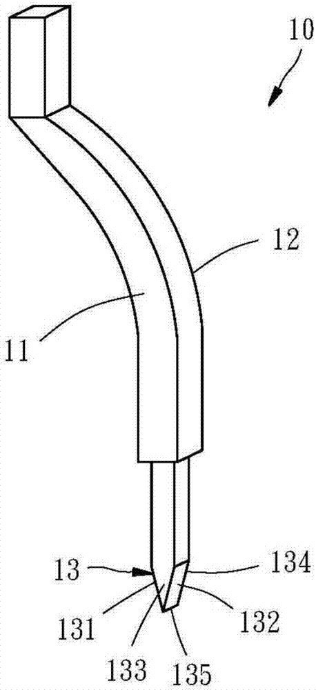
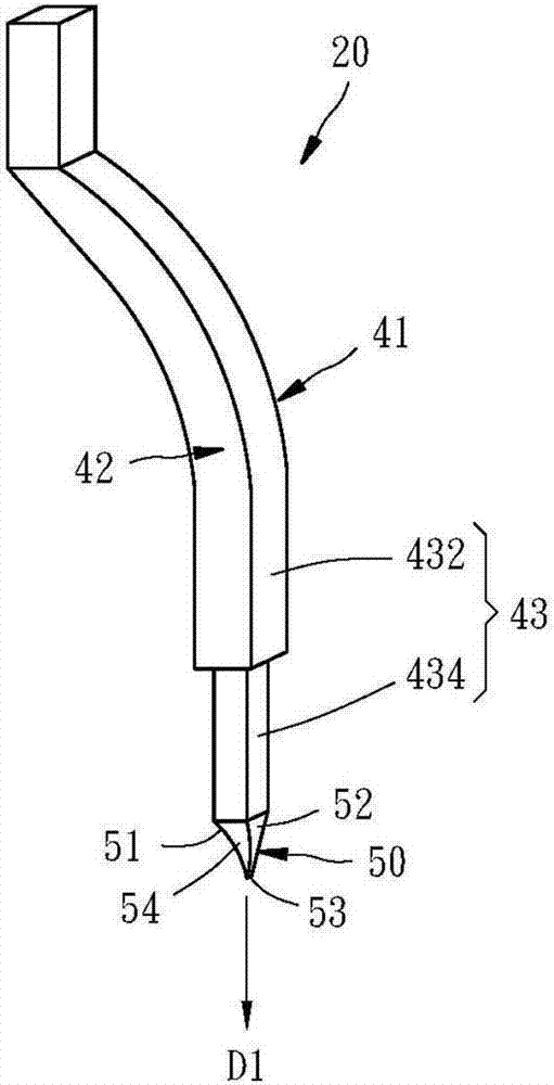
[0048] see figure 2 , the MEMS probe 20 provided by a first preferred embodiment of the present invention is similar to figure 1 The shown buckling probe 10 is conventionally manufactured through the micro-electro-mechanical process, but the design of the tip part is different. The manufacturing method of the micro-electro-mechanical probe 20 will be described below, and the structure of the micro-electro-mechanical probe 20 will also be described. Structure. The manufacturing method of MEMS probe 20 comprises the following steps:

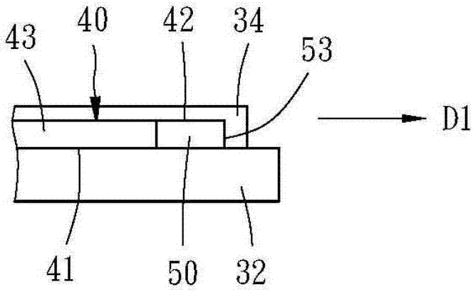
[0049] a) if image 3 As shown, a needle body 40 (as figure 1 As shown in the probe 1...


PUM


Abstract

The invention relates to a microelectromechanical probe. A microelectromechanical probe is manufactured by a MEMS manufacturing process forming a probe body and a cutting process providing a pinpoint portion a cutting face. The probe has a top surface, a body portion, and a pinpoint portion which is substantially extended in a probing direction from the body portion and provided with first and second sides and a probing end substantially oriented in the probing direction. The cutting face is provided on the top surface and descending, adjoins the first and second sides and the probing end, and has at least one cut mark formed by the cutting process. The cut mark is substantially extended from the first side to the second side and non-parallel to the probing direction. The cutting face descends from an edge cut mark to the probing end. As a result, the probing end has a small area, thereby making small probe marks, easily piercing a passivation layer of a device under test, and having more recognizable images.

Description

technical field [0001] The present invention is related to the probe arranged on the probe card for touching the object to be tested, in particular to a micro-electromechanical probe and its manufacturing method, and a probe group structure. Background technique [0002] see figure 1 , figure 1 Shown is a conventional buckling probe 10 (Cobra probe) manufactured by MEMS manufacturing process. not shown), in detail, a photoresist layer is formed on the substrate by photolithography, and the photoresist layer is defined by a mask corresponding to the shape of the front and rear surfaces 11, 12 of the probe 10, The probe 10 is molded in the photoresist layer by electroplating. When the probe 10 is molded, its front and rear surfaces 11 , 12 are parallel to the substrate and assume a horizontal posture. [0003] Compared with the traditional mechanical processing method, the aforementioned micro-electro-mechanical process can produce the probe 10 more quickly, mass-produced i...

Claims


Application Information

Patent Timeline
Patent Type & Authority Applications(China)
IPC IPC(8): G01R1/067
CPCG01R1/06738G01R1/06744G01R3/00B81B1/008B81C1/00007G01R1/07357
Inventor 魏绍伦许育祯沈茂发许志豪
Owner MPI CORP
Why Eureka
Try Eureka