Two dimensional material transverse heterojunction, and preparation and application of the same

A two-dimensional material and heterojunction technology, which is applied in the field of preparation of two-dimensional material lateral heterojunction and its superlattice, can solve the problems of low preparation efficiency, high doping, and too wide interfacial alloy area, and achieve operational The process is simple, the experiment repeatability is good, and the effect of improving atomic level flatness

Active Publication Date: 2017-08-11
HUNAN UNIV
View PDF2 Cites 24 Cited by
  • Summary
  • Abstract
  • Description
  • Claims
  • Application Information

AI Technical Summary

Problems solved by technology

[0012] In order to overcome the problems of high doping between two heterojunction materials, low production efficiency, and excessively wide interface alloy region in the existing heterojunction preparation methods, the present invention provides a two-dimensional material lateral heterojunction The preparation method aims to improve the existing two-dimensional material heterojunction preparation method, so that the horizontal heterojunction of two-dimensional materials with smoothness at the atomic level, steep boundaries, flatness and low doping can be obtained, and high-efficiency preparation can be achieved. The preparation of two-dimensional superlattice solves the problem that the superlattice cannot be obtained simply by growth

Method used


Image

  • Two dimensional material transverse heterojunction, and preparation and application of the same
  • Two dimensional material transverse heterojunction, and preparation and application of the same
  • Two dimensional material transverse heterojunction, and preparation and application of the same

Examples


Embodiment 1

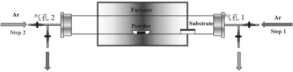
[0094] A method for preparing a lateral heterojunction of a two-dimensional material and a superlattice thereof, the specific implementation steps are as follows:

[0095] (1) Two-dimensional material heterojunction single-component material WS 2 The preparation comprises the following steps:

[0096] Weigh 0.6gWS 2 The powder source is loaded in an alumina boat and placed in the middle high-temperature zone of a tube furnace quartz tube (2 cm diameter). A silicon oxide wafer (Si / 300nmSiO2) is placed in the variable temperature deposition area of ​​the tube furnace as a substrate for material deposition.

[0097] Clean the pipeline with 500 sccm argon gas for 10 minutes in advance, use argon gas as the carrier gas during the heating process, the gas flow rate is 50 sccm respectively, raise the temperature to the growth temperature of 1150 ℃, which is the growth temperature of the growth temperature-related material, and after 5 minutes of growth time, the silicon oxide depos...

Embodiment 2

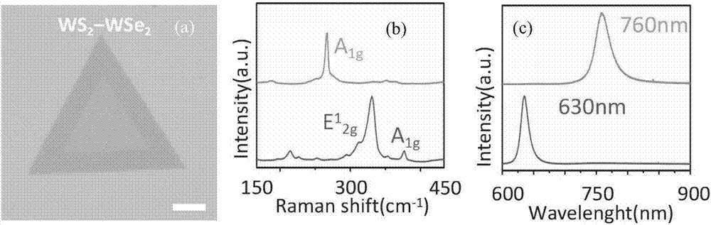
[0104] Compared with Example 1, the difference is that in step (2), the two-dimensional material powder used for lateral epitaxy is MoSe 2 (that is, using MoSe 2 Powder replaces the WSe of embodiment 1 step (2) 2 powder); and MoSe 2 The growth temperature is 1200° C., the growth time is 30 s, and the forward flow Ar flow rate during the growth process is 200 sccm. Prepared two-dimensional material lateral heterojunction WS 2 -MoSe2 .

[0105] image 3 In order to prepare the optical image of the sample, the Raman spectrum test chart, and the fluorescence imaging map, it is confirmed that the obtained sample is free of doping and has excellent performance indicators. image 3 In (a), the scale bar is 5 μm.

Embodiment 3

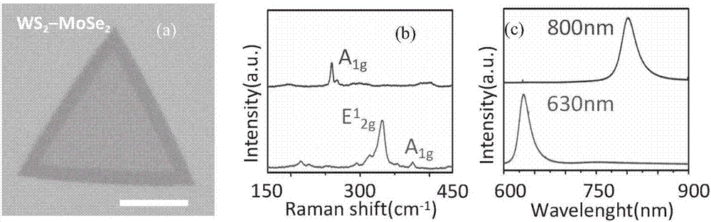
[0107] Compared with Example 1, the difference is that in step (2), the two-dimensional material powder for lateral epitaxy used is MoS 2 (i.e. using MoS 2 Powder replaces the WSe of embodiment 1 step (2) 2 powder); and MoS 2 The growth temperature is 1200° C., the growth time is 2 s, and the forward flow Ar flow rate during the growth process is 300 sccm. Prepared two-dimensional material lateral heterojunction WS 2 -MoS 2 .

[0108] Figure 4 In order to prepare the optical image of the sample, the Raman spectrum test chart, and the fluorescence imaging map, it is confirmed that the obtained sample is free of doping and has excellent performance indicators. Figure 4 In (a), the scale bar is 5 μm.


PUM


Abstract

The invention discloses a preparation method of a two dimensional material transverse heterojunction. The preparation method of a two dimensional material transverse heterojunction includes the following steps: (a), taking material A powder as the original materials, performing vapour deposition on the surface of a substrate, and forming a nanometer sheet of the material A; and (b), heating the powder of the material B1 to the growth temperature under the reverse carrier gas flow, wherein the powder of the material B1 are horizontally growing along the rim of the nanometer sheet of the material A under the positive carrier gas flow, growing in the horizontal direction, and after completion of growing, the reverse carrying gas flow is imported again to prepare a two dimensional material transverse heterojunction A-B1. The invention also provides the two dimensional material transverse heterojunction prepared by the preparation method, and application of the preparation method in preparation of photoelectric devices. The related heterojunction prepared by the preparation method of a two dimensional material transverse heterojunction has the advantages of being smooth in the atomic layer, being steep and flat in the heterojunction boundary line, almost having no doping, and being excellent in optical and electrical properties of the material. The preparation method of a two dimensional material transverse heterojunction greatly simplifies the preparation method of the two dimensional material transverse heterojunction, and controllability of material preparation and the preparation efficiency are greatly improved.

Description

technical field [0001] The invention belongs to the field of nanometer materials, and relates to a preparation method of a two-dimensional material lateral heterojunction and a superlattice thereof. [0002] technical background [0003] In the field of two-dimensional materials, the discovery of graphene in 2004 first triggered a research boom, but due to the special zero-gap energy band structure of graphene, it has been greatly limited in the fields of electronics and optoelectronics, such as graphene field effect transistors. The switching ratio is very small, limiting its use in logic circuits. While B. Radisavljevic et al. use single-layer MoS 2 The prepared field effect transistor has a switch ratio as high as 10 8 , with great application prospects, with single-layer MoS 2 The new two-dimensional materials represented by [1] . [0004] Layered materials such as TMDs have the same layered structure characteristics as graphite. The atoms in the layers are bonded by...

Claims


Application Information

Patent Timeline
Patent Type & Authority Applications(China)
IPC IPC(8): H01L21/383H01L29/06H01L29/15H01L29/24H01L31/032H01L31/0352H01L33/06H01L33/26H01S5/30H01S5/32H01S5/34B82Y30/00B82Y40/00
Inventor 段镶锋段曦东张正伟陈鹏
Owner HUNAN UNIV
Why Eureka
Try Eureka