Preparation method of topological insulator Bi2Se3/FeSe2 alloplasmic structure thin film

A technology of topological insulators and heterostructures, applied in the field of preparation of heterostructure thin films, can solve the problems of uneven coating process of heterostructure thin films, poor reproducibility of heterostructure thin films, and high preparation costs, so as to reduce preparation costs , good combination and reduced equipment requirements

Active Publication Date: 2017-08-18
SOUTHWEST JIAOTONG UNIV
View PDF5 Cites 9 Cited by
  • Summary
  • Abstract
  • Description
  • Claims
  • Application Information

AI Technical Summary

Problems solved by technology

Molecular beam epitaxy (MBE) technology requires high vacuum, high-purity gas, and expensive equipment, and its preparation cost is high
The heterostructure thin film formed by evaporation coating technology is uneven and the coating process is complicated, and the repeatability of heterostructure thin film preparation is poor

Method used


Image

  • Preparation method of topological insulator Bi2Se3/FeSe2 alloplasmic structure thin film
  • Preparation method of topological insulator Bi2Se3/FeSe2 alloplasmic structure thin film
  • Preparation method of topological insulator Bi2Se3/FeSe2 alloplasmic structure thin film

Examples


Embodiment 1

[0025] A topological insulator Bi 2 Se 3 / FeSe 2 A method for preparing a heterostructure thin film, the steps of which are:

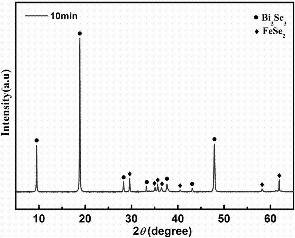
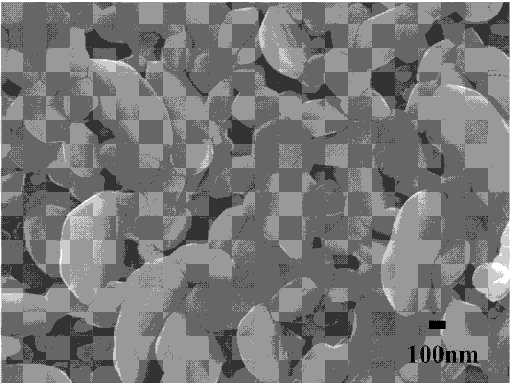
[0026] a, the preparation of FeSe base film: take FeSe material as target material, form FeSe base film by magnetron sputtering on Si(100) substrate; The specific method of described magnetron sputtering is: the distance between substrate and target material The vacuum chamber of the magnetron sputtering equipment is evacuated to an air pressure of less than 2×10 -4 Pa, and then pass in analytically pure argon to make the pressure of the vacuum chamber 0.5Pa, adjust the substrate temperature to 420°C, and the sputtering power density to 3.31W / cm 2 , the sputtering time is 10min;

[0027] b. FeSe 2Annealing and phase formation: the substrate obtained in step a with the FeSe base film sputtered and selenium particles are sealed together with an air pressure of less than 1×10 -2 In the vacuum quartz tube of Pa, put the vacuum quartz tube in the heat...

Embodiment 2

[0035] A topological insulator Bi 2 Se 3 / FeSe 2 A method for preparing a heterostructure thin film, the steps of which are:

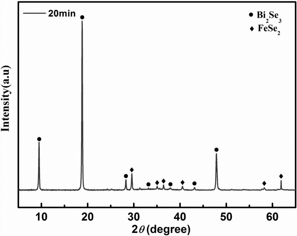
[0036] a, the preparation of FeSe base film: take FeSe material as target material, form FeSe base film by magnetron sputtering on Si(100) substrate; The specific method of described magnetron sputtering is: the distance between substrate and target material 6cm, the vacuum chamber of the magnetron sputtering equipment is evacuated to an air pressure of less than 2×10 -4 Pa, and then pass in analytically pure argon to make the pressure of the vacuum chamber 0.4Pa, adjust the substrate temperature to 400°C, and the sputtering power density to 3.05W / cm 2 , the sputtering time is 20min;

[0037] b. FeSe 2 Annealing and phase formation: the substrate obtained in step a with the FeSe base film sputtered and selenium particles are sealed together with an air pressure of less than 1×10 -2 In the vacuum quartz tube of Pa, put the vacuum quartz tube in th...

Embodiment 3

[0045] A topological insulator Bi 2 Se 3 / FeSe 2 A method for preparing a heterostructure thin film, the steps of which are:

[0046] a, the preparation of FeSe base film: take FeSe material as target material, form FeSe base film by magnetron sputtering on Si(100) substrate; The specific method of described magnetron sputtering is: the distance between substrate and target material 7cm, the vacuum chamber of the magnetron sputtering equipment is evacuated to an air pressure of less than 2×10 -4 Pa, and then pass in analytically pure argon to make the pressure of the vacuum chamber 0.6Pa, adjust the substrate temperature to 380°C, and the sputtering power density to 2.80W / cm 2 , the sputtering time is 30min;

[0047] b. FeSe 2 Annealing and phase formation: the substrate obtained in step a with the FeSe base film sputtered and selenium particles are sealed together with an air pressure of less than 1×10 -2 In the vacuum quartz tube of Pa, put the vacuum quartz tube in th...


PUM


Abstract

The invention discloses a preparation method of a topological insulator Bi2Se3/FeSe2 alloplasmic structure thin film. The preparation method includes the main steps that a, a FeSe base film is prepared, wherein the FeSe base film is formed on a base sheet through magnetron sputtering; b, FeSe2 annealing phase forming is carried out, wherein the base sheet obtained in the step a and selenium particles are sealed into a vacuum quartz tube with the air pressure smaller than 1*10<-2> Pa, annealing phase forming treatment is carried out, and an FeSe2 thin film is obtained on the base sheet; c, a Bi2Se3 base film is prepared, wherein on the base sheet obtained in the step b, magnetron sputtering is carried out to form a Bi2Se3 film, and then a Bi2Se3/FeSe2 base film is formed on the base sheet; and d, Bi2Se3 annealing phase forming is carried out, wherein the base sheet obtained in the step c and selenium particles are sealed into a vacuum quartz tube with the air pressure small than 1*10<-2> Pa, annealing phase forming treatment is carried out, and the product is obtained. According to the method, the film coating amount is easily controlled, the formed alloplasmic structure thin film is smooth and good in performance. The preparing cost is low.

Description

technical field [0001] The invention relates to a preparation method of a topological insulator material, in particular to a preparation method of a heterogeneous structure film of a topological insulator. Background technique [0002] A topological insulator is a type of insulator that is different from ordinary insulators. Its body is insulating like the insulators that people usually recognize; however, there are always conductive edge states on its boundary or surface, which is different from ordinary insulators. most unique properties. This unique property is called "topological" symmetry, that is, the surface of the topological insulator is continuously removed, and the new surface that appears is always a conductive edge state. That is to say, the conductive edge states on the surface are stable. The reason is that the strong spin-orbit coupling of electrons forms a conductive surface state that has no energy gap, no dissipation, and is not easily damaged by defects...

Claims


Application Information

Patent Timeline
Patent Type & Authority Applications(China)
IPC IPC(8): C23C14/35C23C14/06C23C14/58
CPCC23C14/0623C23C14/35C23C14/5806
Inventor 郑良雷鸣金荣羊新胜张勇赵勇
Owner SOUTHWEST JIAOTONG UNIV
Why Eureka
Try Eureka