Display device and manufacturing method therefor

A technology for display devices and liquid crystal layers, applied in instruments, optics, nonlinear optics, etc., can solve problems such as complex drive circuits, and achieve the effects of increased transmittance and reduced manufacturing costs

Inactive Publication Date: 2017-08-18
SAMSUNG ELECTRONICS CO LTD
View PDF6 Cites 9 Cited by
  • Summary
  • Abstract
  • Description
  • Claims
  • Application Information

AI Technical Summary

Problems solved by technology

However, the latter display device may have a complicated driving circuit because different driving voltages are applied to the liquid crystals of the R, G, and B pixels

Method used


Image

  • Display device and manufacturing method therefor
  • Display device and manufacturing method therefor
  • Display device and manufacturing method therefor

Examples


Embodiment 1

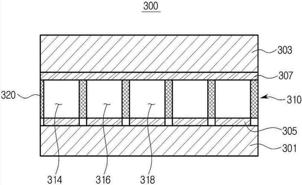
[0150] The cholesteric liquid crystal, the monomer, and the photosensitive chiral dopant were mixed in a weight ratio of 84.5:12.5:3.0. As the cholesteric liquid crystal, CH100-650 available from Slichem was used.

[0151] The birefringence of CH100-650 was 1.66 for ne (main axis) and 1.502 for no (longitudinal axis (vertical axis)), and its dielectric anisotropy was 27.8. The monomer may include an acrylate monomer, a crosslinking agent, and a photopolymerization initiator mixed in a weight ratio of 90:9:1. The monomers are isotropic at room temperature. As the photosensitive chiral dopant, methoxy-cinnamoyl glucitol was used. Methoxy-cinnamoyl glucitol reacts with UV light having a wavelength of about 350 nm or less.

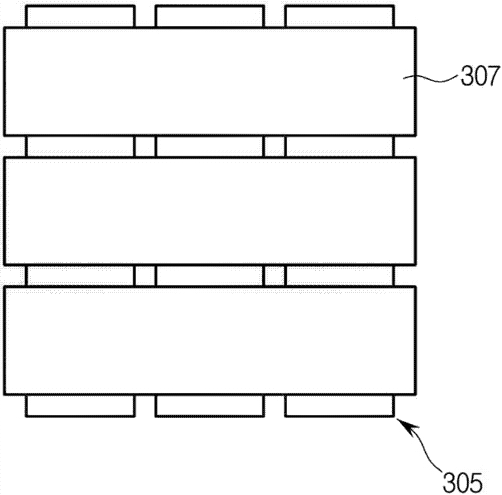
[0152] The mixture was coated on a polycarbonate plastic substrate coated with lithium zinc oxide to form a liquid crystal layer 310, and the liquid crystal layer 310 was exposed by using a UV bandpass filter with a bandwidth of 355-370 nm available from Ed...


PUM


Abstract

Provided are a display device having the same operating voltage per pixel and a manufacturing method therefor. The display device according to one aspect comprises: a first substrate; a second substrate; and a liquid crystal layer which is placed between the first substrate and the second substrate and has a plurality of sub-cells, wherein the plurality of sub-cells comprise a hardened polymer to secure cholesteric liquid crystal and a spiral pitch of the cholesteric liquid crystal.

Description

technical field [0001] The present disclosure relates to a display device in which the same driving voltage is applied to pixels and a method of manufacturing the same. Background technique [0002] A display device is a device for displaying visual and stereoscopic image information. Recently, flat display devices having excellent properties such as high image quality have been developed. [0003] Examples of flat display devices include thin film transistor liquid crystal display devices (TFT-LCD) and liquid crystal display devices (LCD). These display devices can be classified into transmissive display devices and reflective display devices. [0004] The TFT-LCD, which is a transmissive liquid crystal display device, includes a light source for backlight disposed under a lower substrate, which consumes a large amount of power (electric power). [0005] Thus, cholesteric (cholesteric) liquid crystal display devices have been developed as reflective display devices. A c...

Claims


Application Information

Patent Timeline
Patent Type & Authority Applications(China)
IPC IPC(8): G02F1/137G02F1/1334
CPCG02F1/133377G02F1/13718G02F2202/06G02F1/13775G02F1/13345G02F1/1334G02F1/1341G02F2201/52G02F2202/023
Inventor 卢禧烈权纯凡金景善金雁金朱镐李范荣郑俊诚
Owner SAMSUNG ELECTRONICS CO LTD
Why Eureka
Try Eureka