Modification method for flip-chip packaging integrated circuit

An integrated circuit and flip-chip technology, applied in the field of modification of integrated circuits, can solve the problem of inability to observe the chip structure, and achieve the effect of meeting thickness requirements, high thinning precision and high efficiency

Inactive Publication Date: 2017-08-25
CHINA ELECTRONICS PROD RELIABILITY & ENVIRONMENTAL TESTING RES INST
View PDF7 Cites 5 Cited by
  • Summary
  • Abstract
  • Description
  • Claims
  • Application Information

AI Technical Summary

Problems solved by technology

The flip-chip (initial thickness is about a few hundred microns thick) package faces down, and the circuit is located under the chip. The traditional FIB modification technology cannot observe the internal structure of the chip through the back of the silicon chip, let alone determine the target position and carry out the circuit. edited
However, due to the electrical, thermal and other characteristics of the chip package, a complete circuit error correction test can only be performed after the chip is packaged, and the wafer-level test can only achieve basic test functions.

Method used


Image

  • Modification method for flip-chip packaging integrated circuit
  • Modification method for flip-chip packaging integrated circuit
  • Modification method for flip-chip packaging integrated circuit

Examples


Embodiment

[0044] This embodiment is a method for modifying a circuit of a flip-chip packaged integrated circuit. The integrated circuit includes a substrate and a chip that is flip-chip packaged on the substrate. area.

[0045] The circuit modification method includes the steps of:

[0046] (1) Grinding the chip, reducing the original thickness of the chip from 393 μm to 70-80 μm; specifically, the grinding method is: firstly use diamond abrasive paper with a particle size of 25-35 μm for rough grinding; Finely grind with diamond abrasive paper with a diameter of 10-20 μm; then polish with a diamond suspension with a particle size of 4-8 μm and a polishing cloth, and then polish and fine-grind with a diamond suspension with a particle size of 0.5-2 μm and a flocking cloth;

[0047] (2) Using FIB combined with etching auxiliary gas (such as XeF 2 ) performing the first etching on the chip after grinding, and thinning the chip to about 4 μm;

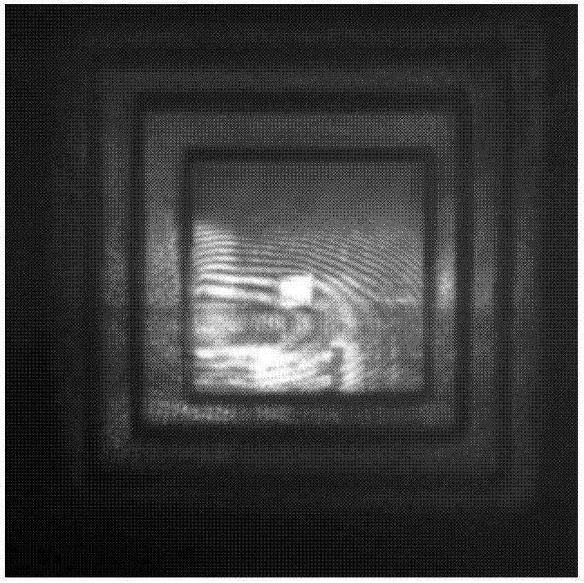
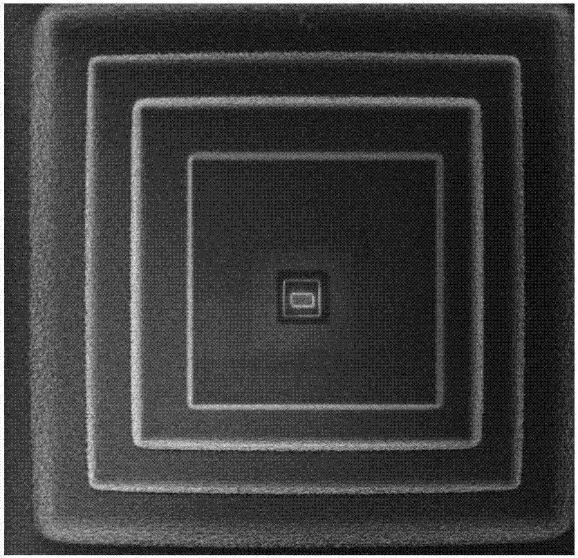
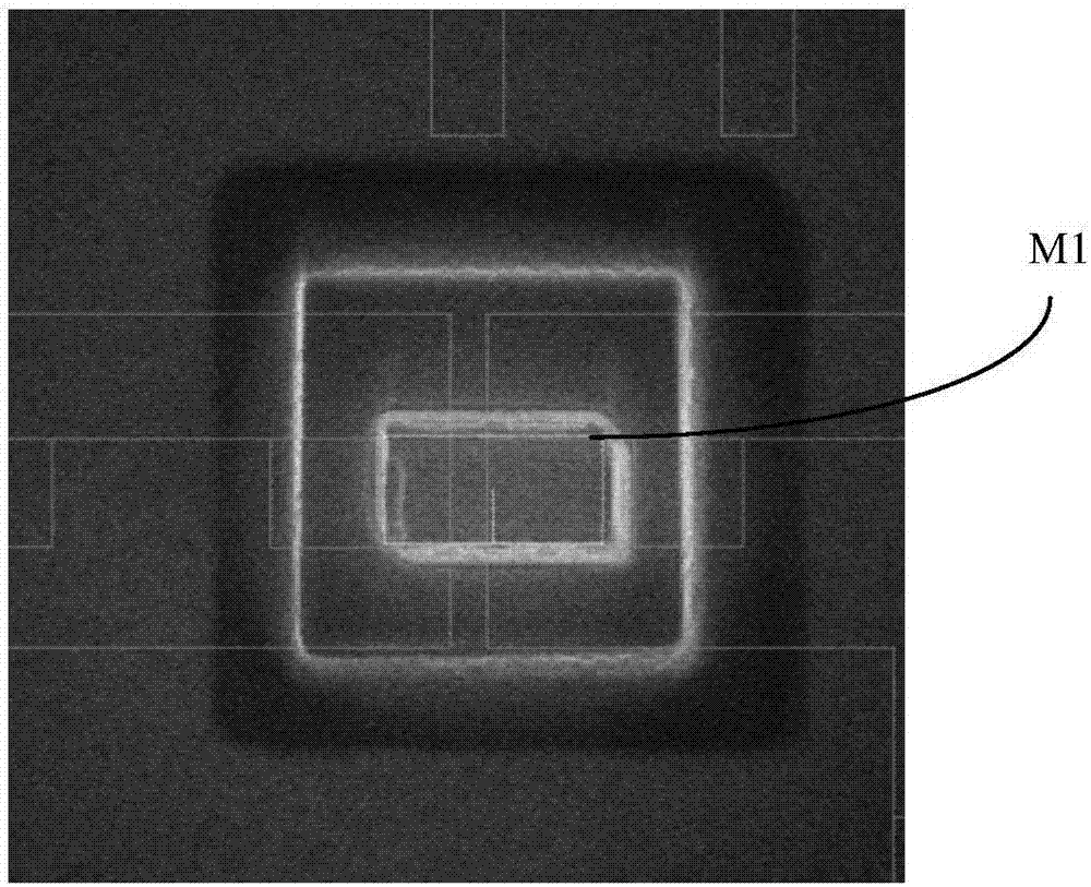
[0048] (3) Imaging the chip after etching, a...


PUM


Abstract

The invention relates to a circuit modification method for a flip-chip packaging integrated circuit. The integrated circuit comprises a substrate, and a chip packaged on the substrate in a flip-chip mode, and a surface of the chip fitting the substrate has a to-be-modified region. The method comprises steps that (1), the chip is ground; (2), first etching for the chip after grinding is carried out through employing a focusing ion beam in combination with an auxiliary etching gas; (3), imaging of the chip after etching is carried out, and the position of the to-be-modified region is determined according to a circuit image acquired through imaging; (4), second etching for the chip after the first etching is carried out through employing the focusing ion beam in combination with the auxiliary etching gas, and the to-be-modified region is exposed; a circuit of the to-be-modified region is modified through utilizing the focusing ion beam. The method is advantaged in that circuit modification for the chip employing flip-chip packaging can be carried out, and circuit modification efficiency is high.

Description

technical field [0001] The present invention relates to integrated circuits, and more particularly to methods of modifying flip-chip packaged integrated circuits. Background technique [0002] After the design of the chip is completed and the chip is released, the success rate of the chip cannot be guaranteed to be 100%. It is usually necessary to perform a failure analysis on the problematic (ie failed) chip to find out the cause of the failure. If the failure is caused by the chip design, it is necessary to modify the circuit of the chip, that is, to use the circuit modification error correction function of the focused ion beam (FIB), to partially section the sample, and partially deposit metal and dielectric layers. Modify the device layout of the multilayer wiring structure, and then perform functional verification to confirm whether the modification is successful. If successful, correct the design error and re-strip. [0003] At present, the processing method of FIB is...

Claims


Application Information

Patent Timeline
Patent Type & Authority Applications(China)
IPC IPC(8): H01L21/66H01L21/304H01L21/3065
CPCH01L21/304H01L21/3065H01L22/24
Inventor 林晓玲陈立辉章晓文陈义强
Owner CHINA ELECTRONICS PROD RELIABILITY & ENVIRONMENTAL TESTING RES INST
Why Eureka
Try Eureka