
SCR for electrostatic protection, chip and system

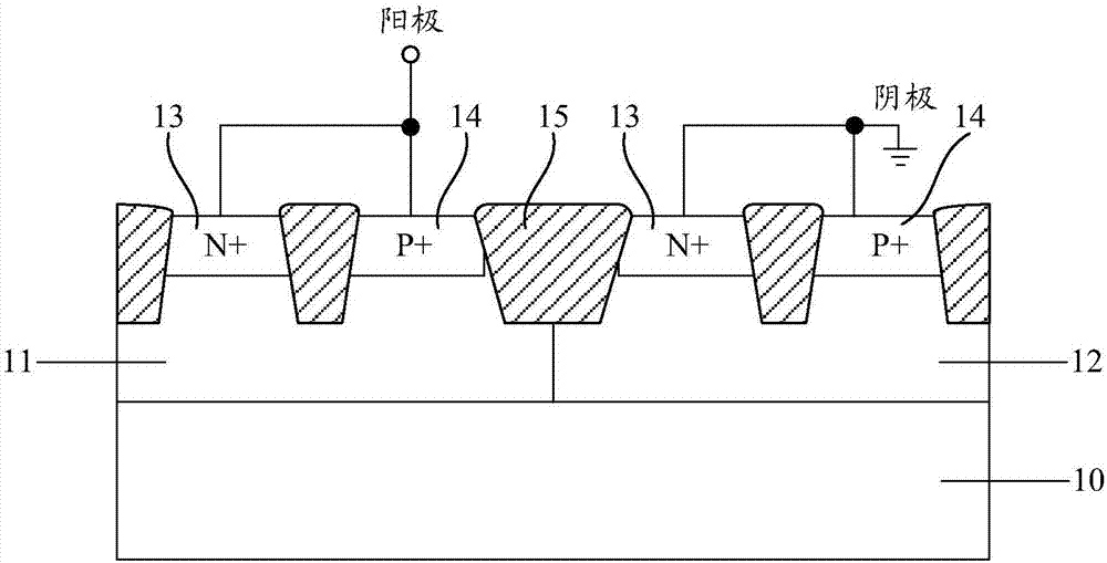
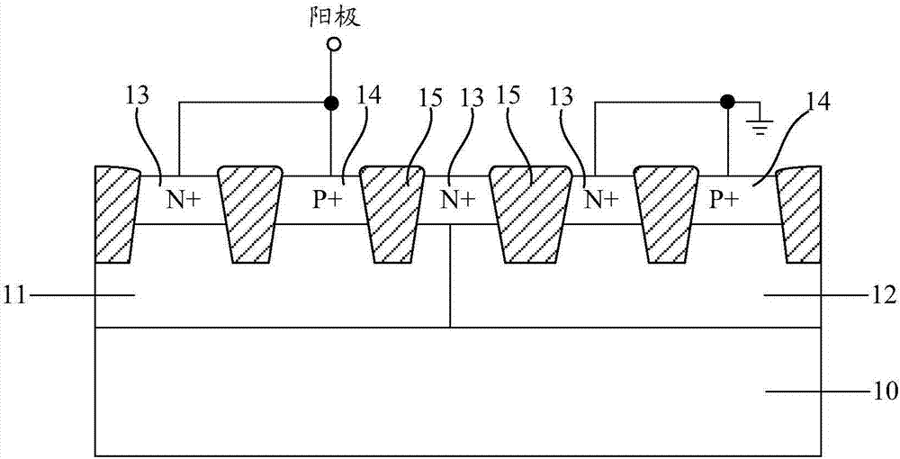
An electrostatic protection and chip technology, applied in the electronic field, can solve problems such as unsatisfactory and ineffective reduction of static electricity impact on internal circuits.

Inactive Publication Date: 2017-08-25
HUAWEI TECH CO LTD
View PDF3 Cites 7 Cited by
  • Summary
  • Abstract
  • Description
  • Claims
  • Application Information

AI Technical Summary

Problems solved by technology

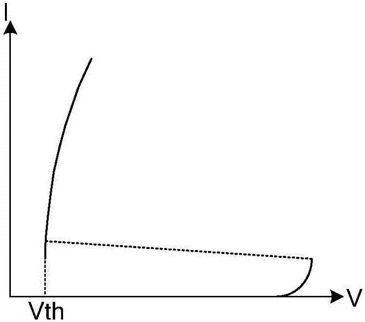
This improvement can reduce the turn-on voltage to about 12V and maintain the voltage at about 1.5V (such as Figure 4 As shown), but still can not meet these protocol interfaces such as High Definition Multimedia Interface (High Definition Multimedia Interface, HDMI), Universal Serial Bus (Universal Serial Bus, USB), Video Interface (Video-By-One, VBO) etc. needs
Because, on the one hand, the power supply voltage of these interfaces is generally around 3.3V, and the maintenance voltage of 1.5V is much lower than 3.3V, which will cause latch-up effect; on the other hand, the additional board-level transient suppression (Transient Voltage The turn-on voltage of the Suppressor (TVS) diode is about 8-10V, and the turn-on voltage of 12V cannot effectively reduce the impact or even damage of the internal circuit caused by static electricity.

Method used


Image

  • SCR for electrostatic protection, chip and system
  • SCR for electrostatic protection, chip and system
  • SCR for electrostatic protection, chip and system

Examples


Embodiment 1

[0051] Embodiment 1 provides an SCR for electrostatic protection, such as Figure 6 As shown, it includes a semiconductor substrate 10, an N-type first well 21 located on the semiconductor substrate 10, a P-type second well 22, and an N-type third well 23. The second well 22 is located between the first well 21 and the third well. Between 23.

[0052] The N-type first well 21 is provided with an N-type first heavily doped region 31 and a P-type second heavily doped region 32 .

[0053] The N-type third well 23 is provided with an N-type third heavily doped region 33 .

[0054] The P-type second well 22 is provided with a P-type fourth heavily doped region 34, and the P-type fourth heavily doped region 34 extends to the first well 21 and the third well 23; the P-type fourth heavily doped region 34 and There is a first interval (denoted as L1 ) between the P-type second heavily doped regions 32 , and metal gates 41 are arranged at the first interval.

[0055] Wherein, the fir...

Embodiment 2

[0066] Embodiment two, provide a kind of SCR that is used for electrostatic protection, such as Figure 8 As shown, it includes a semiconductor substrate 10, a P-type first well 21 located on the semiconductor substrate 10, an N-type second well 22, and a P-type third well 23. The second well 22 is located between the first well 21 and the third well. Between 23.

[0067] The P-type first well 21 is provided with a P-type first heavily doped region 31 and an N-type second heavily doped region 32 .

[0068] The P-type third well 23 is provided with a P-type third heavily doped region 33 .

[0069] N-type second well 22 is provided with N-type fourth heavily doped region 34, N-type fourth heavily doped region 34 extends to first well 21 and third well 23; N-type fourth heavily doped region 34 and There is a first interval L1 (denoted as L1 ) between the N-type second heavily doped regions 32 , and metal gates 41 are disposed at the first interval.

[0070] Wherein, the first ...

Embodiment 3

[0088] Embodiment three, provide a kind of SCR that is used for electrostatic protection, such as Figure 10 As shown, it includes a semiconductor substrate 10 , an N-type fourth well 24 , a P-type fifth well 25 and an N-type sixth well 26 located on the semiconductor substrate 10 .

[0089] A P-type fifth heavily doped region 35 is disposed in the N-type fourth well 24 .

[0090] The P-type fifth well 25 is provided with an N-type sixth heavily doped region 36 and an N-type seventh heavily doped region 37, the N-type sixth heavily doped region 36 extends into the fourth well 24, and the N-type seventh heavily doped region 37 extends into the fourth well 24. The heavily doped region 37 extends into the sixth well 26 ; there is a second distance (denoted as L2 ) between the sixth heavily doped region 36 and the seventh heavily doped region 37 , and a metal gate 41 is disposed at the second distance.

[0091] Wherein, the fifth heavily doped region 35 and the sixth heavily dope...


PUM


Abstract

The invention provides a semiconductor controlled rectifier (SCR) for electrostatic protection, a chip and a system, relates to the electronic technology field and can realize start voltage reduction and maintenance voltage improvement. The SCR comprises a semiconductor substrate, and a first well, a second well and a third well which are arranged on the semiconductor substrate, wherein conductive types of the first well and the third well are identical, the second well is in a different conductive type, the first well is internally provided with a first heavily doped region and a second heavily doped region, the first heavily doped region and the second heavily doped region are different in conductive types, the first heavily doped region and the first well are identical in conductive types, the third well is internally provided with a third heavily doped region, the third heavily doped region and the third well are identical in conductive types, the second well is internally provided with a fourth heavily doped region, the four heavily doped region and the second well are identical in conductive types, the fourth heavily doped region extends to the first well and the third well, a first gap is arranged between the fourth heavily doped region and the second heavily doped region, and a metal gate is arranged at the first gap.

Description

technical field [0001] The present application relates to the field of electronic technology, in particular to an SCR, a chip and a system for electrostatic protection. Background technique [0002] Electrostatic Discharge (ESD) is a common natural phenomenon in our life, but the large current generated by ESD in a short period of time can cause fatal damage to integrated circuits (Integrated Circuit, IC). For example, for the electrostatic discharge phenomenon (Human-Body Model, HBM) that occurs in the human body, it usually occurs within hundreds of nanoseconds, and the maximum current peak value may reach several amperes. Some other modes, such as machine discharge mode (MachineModel, MM) and component charging mode (Charged-Device Model, CDM), have shorter electrostatic discharge time and larger current. Such a large current passes through the IC in a short time, and the power consumption generated will seriously exceed the maximum value it can withstand, which will cau...

Claims


Application Information

Patent Timeline
IPC IPC(8): H01L23/60H01L27/02
CPCH01L23/60H01L27/0248
Inventor 刘悦李江宏李斌俞恢春
Owner HUAWEI TECH CO LTD
Learn More