Supercharge Your Innovation With Domain-Expert AI Agents!

Electronic element and preparation method thereof

A technology for electronic components and gate electrodes, applied in the field of electronic components and their preparation, can solve problems such as low breakdown voltage, and achieve the effects of increasing the breakdown voltage, reducing the on-resistance, and increasing the average electric field

Pending Publication Date: 2017-09-05
工业和信息化部电子第五研究所华东分所
View PDF6 Cites 0 Cited by
  • Summary
  • Abstract
  • Description
  • Claims
  • Application Information

AI Technical Summary

Problems solved by technology

[0004] In view of this, an embodiment of the present invention provides an electronic component and its preparation method to solve the technical problem of low breakdown voltage of electronic components in the prior art

Method used


Image

  • Electronic element and preparation method thereof
  • Electronic element and preparation method thereof
  • Electronic element and preparation method thereof

Examples


Embodiment Construction

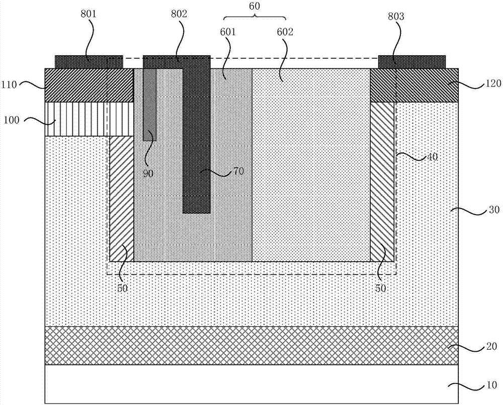
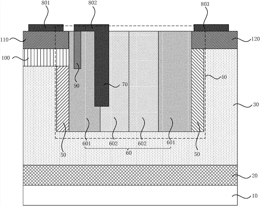
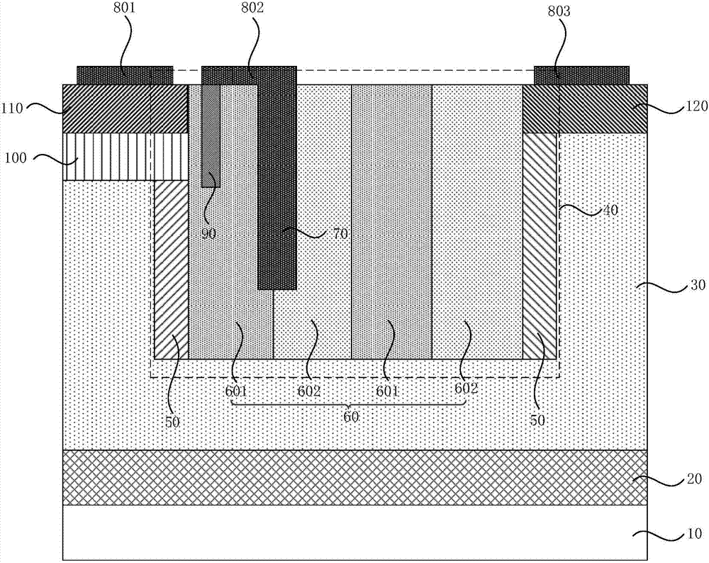
[0052] In order to make the purpose, technical solution and advantages of the present invention clearer, the technical solution of the present invention will be fully described below through specific implementation in combination with the drawings in the embodiments of the present invention. Apparently, the described embodiments are some embodiments of the present invention, rather than all embodiments. Based on the embodiments of the present invention, all other embodiments obtained by persons of ordinary skill in the art without making creative efforts, All fall within the protection scope of the present invention.

[0053] figure 1 is a schematic structural diagram of an electronic component provided by an embodiment of the present invention, such as figure 1 As shown, the electronic components provided by the embodiments of the present invention may include:

[0054]Substrate 10;

[0055] A buried oxide layer 20 located on the substrate 10;

[0056] The drift layer 30 ...


PUM


Abstract

An embodiment of the invention discloses an electronic element and a preparation method thereof. The electronic element includes a substrate; a buried oxide layer located on the substrate; a drift layer located on the buried oxide layer and formed with a window in the upper surface; a doped region located on the inner wall of the window or on the inner wall and lower surface of the window; an insulating layer located in the window and composed of at least one first insulating layer and at least one second insulating layer; a metal field plate located in the insulating layer and arranged corresponding to the doped region; and source, gate and drain electrodes located on a side, far from the buried oxide layer, on the drift layer or the insulating layer. With the above technical scheme, an electric field peak value is introduced to an interface junction between the first insulating layer and the second insulating layer, an electric field peak value is introduced to the metal field plate, the average electric field of the drift layer can be enhanced, and the breakdown voltage of the electronic element is improved.

Description

technical field [0001] The invention relates to the technical field of electronic components, in particular to an electronic component and a preparation method thereof. Background technique [0002] Power integrated circuits, also known as high-voltage integrated circuits, are an important branch of modern electronics. They can provide new circuits with high speed, high integration, low power consumption and radiation resistance for various power conversion and energy processing devices, and are widely used in power control. Systems, automotive electronics, display device drivers, communications and lighting and other daily consumer fields, as well as many important fields such as national defense and aerospace. The rapid expansion of its application scope has also put forward higher requirements for the high-voltage devices in its core part. For power devices, on the premise of ensuring the breakdown voltage, the on-resistance of the device must be reduced as much as possi...

Claims


Application Information

Patent Timeline
IPC IPC(8): H01L29/06H01L29/40H01L29/78H01L21/336
CPCH01L29/0611H01L29/402H01L29/66674H01L29/7816
Inventor 夏超张琦吴良松陈锃基
Owner 工业和信息化部电子第五研究所华东分所
Features
  • R&D
  • Intellectual Property
  • Life Sciences
  • Materials
  • Tech Scout
  • Unparalleled Data Quality
  • Higher Quality Content
  • 60% Fewer Hallucinations
Learn More