Electromagnetic-field near-field PCB probe

An electromagnetic field and near-field technology, applied in the field of measurement probes, can solve the problems of environmental temperature influence, unstable measurement accuracy and sensitivity, achieve stable anti-temperature interference ability, good measurement repeatability and stability, and improve the degree of anti-interference. Effect

Inactive Publication Date: 2017-09-08
HEBEI UNIV OF TECH
View PDF8 Cites 7 Cited by
  • Summary
  • Abstract
  • Description
  • Claims
  • Application Information

AI Technical Summary

Problems solved by technology

[0004] The technical problem to be solved by the present invention is to provide an electromagnetic field near-field PCB probe, which is an electromagnetic field near-field PCB probe with temperature compensation. The structure adjusts the temperature-capacitance parameters, which overcomes the defects that the existing electromagnetic field near-field PCB probes are easily affected by the ambient temperature, and the measurement accuracy and sensitivity are unstable.

Method used


Image

  • Electromagnetic-field near-field PCB probe
  • Electromagnetic-field near-field PCB probe
  • Electromagnetic-field near-field PCB probe

Examples


Embodiment

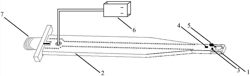
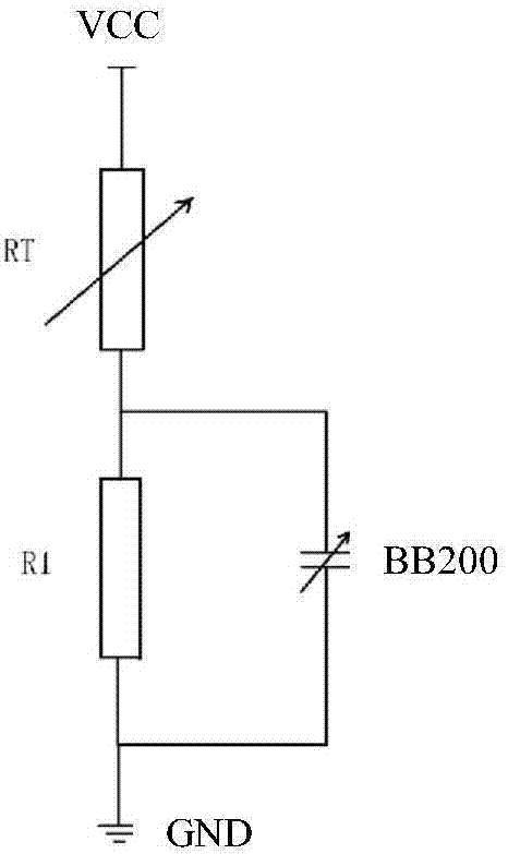
[0032]An electromagnetic field near-field PCB probe of this embodiment is an electromagnetic field near-field PCB probe with temperature compensation, and its composition is as described above figure 1 The illustrated embodiment includes embedded stripline 1, four-layer PCB printed circuit board 2, negative temperature coefficient thermistor 3, voltage divider resistor 4, varactor diode 5, 2V DC power supply 6 and SMA terminal 7; the above The connection method of the components is: the 2V DC voltage provided by the 2V DC power supply 6 is added to the series circuit composed of the negative temperature coefficient thermistor 3 and the voltage dividing resistor 4, and the connection point of the negative temperature coefficient thermistor 3 and the voltage dividing resistor 4 It is a voltage dividing point, which is connected to the negative pole of the varactor diode 5, and the anode of the varactor diode 5 is connected to the copper ground on the surface of the four-layer PCB...


PUM


Abstract

The invention provides an electromagnetic-field near-field PCB probe, which relates to the measuring probe to measure electromagnetic variables and serves as an electromagnetic-field near-field PCB probe with temperature compensation. The probe is structured by an embedded type strip line, a four-layer PCB, a negative temperature coefficient thermal resistor, a voltage division resistor, a variable capacitance diode, a 2V direct current power supply and an SMA terminal. Through the use of the thermal resistor, the variable capacitance diode and the voltage division resistor to adjust the temperature-capacitance parameters for the strip line structure of the probe, it is possible to overcome the defects of a currently available electromagnetic-field near-field PCB probe that the probe is prone to be influenced by environmental temperature, and that the measuring precision and sensitivity are not stable enough.

Description

technical field [0001] The technical solution of the invention relates to a measuring probe for measuring electromagnetic variables, in particular to an electromagnetic field near-field PCB probe. Background technique [0002] New technologies and new equipment for near-field detection of electromagnetic fields emerge in an endless stream. In the actual measurement process, the test equipment for electromagnetic field near-field detection is easily disturbed by the surrounding environment. In addition to the inherent characteristics of the equipment itself, the ambient temperature has a great influence on the sensing equipment and materials, especially the PCB circuit substrate and electromagnetic field. Near-field PCB probes. In the range of ambient temperature from 0 to 80 degrees Celsius, the variation range of the dielectric constant of the PCB material can reach more than 10%. In the actual test environment, the temperature distribution on the surface of circuit board...

Claims


Application Information

Patent Timeline
Patent Type & Authority Applications(China)
IPC IPC(8): G01R29/08
CPCG01R29/0878
Inventor 李尔平宋涛李伶研
Owner HEBEI UNIV OF TECH
Why Eureka
Try Eureka