Active frequency selection surface with broadband and angle stability
A frequency selective surface and angle technology, which is applied in the microwave field, can solve the problems of limiting the use occasion and practicability of the frequency selective surface, the inability to take into account the angle stability, and the influence of the performance of the frequency selective surface, etc., to achieve simple and easy processing and structure The Effects of Simplicity, Reduced Complexity and Cost
- Summary
- Abstract
- Description
- Claims
- Application Information
AI Technical Summary
Problems solved by technology
Method used
Image
Examples
Embodiment 1
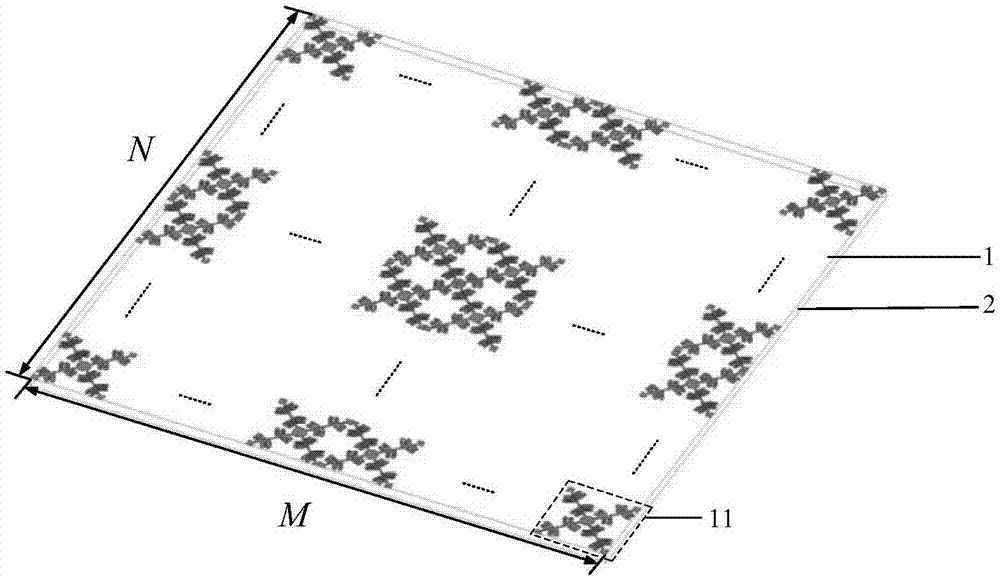
[0020] Reference figure 1 with figure 2 , The present invention includes:
[0021] Periodic surface 1 and dielectric substrate 2. Periodic surface 1 is located on the upper surface of dielectric substrate 2. It consists of M×N square active resonant units 11 with side length p=20mm arranged periodically with side length p, where M =15, N=15, the relative permittivity of the dielectric substrate 2 ε'= 2.20, the electrical loss tangent tanδ D = 0.0007, thickness t = 0.8mm.
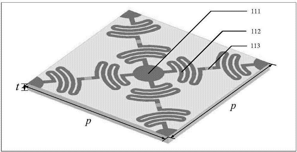
[0022] Each active resonant unit 11 is composed of a circular patch 111, a deformed X-shaped patch 112, and a varactor 113. The circular patch 111 and the deformed X-shaped patch 112 are located at the center, and the circular patch 111 It coincides with the center point of the deformed X-shaped patch 112, and each of the four ends of the deformed X-shaped patch 112 is connected to a varactor 113. The radius of the circular patch 111 is r=1 mm.
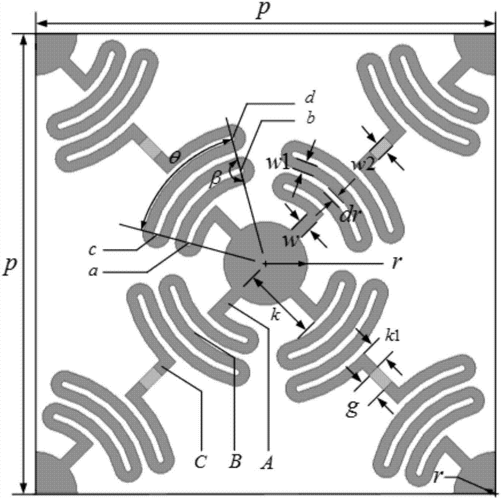
[0023] Reference image 3 , The deformed X-shaped patch 112 is comp...
Embodiment 2
[0026] The structure of this embodiment is the same as that of embodiment 1, and only the following parameters are adjusted:
[0027] The thickness of the dielectric substrate 2 is t=0.75mm, the length of the first straight section A is k=3.4mm, and the width w=0.5mm; the opening angle of the fan-shaped hairpin line is θ=60 ° , The bending angle is β=175°, the width of the fan-shaped hairpin line w1=0.4mm, the bending interval of the fan-shaped hairpin line dr=0.2mm; the length of the second straight line segment B k1=0.7mm, the width is the same as the first straight line segment A Same; the capacitance of the varactor is 0.1pf~1.0pf, the change step is 0.15pf, the length g=0.8mm, and the width w2=0.4mm.
Embodiment 3
[0029] The structure of this embodiment is the same as that of embodiment 1, and only the following parameters are adjusted:
[0030] The thickness of the dielectric substrate 2 is t = 1.05 mm, the length of the first straight line A is k = 3.6 mm, and the width w = 0.7 mm; the opening angle of the fan-shaped hairpin line is θ = 65°, the bending angle is β = 185°, the fan-shaped hairpin The width of the line w1=0.6mm, the bending interval of the fan-shaped hairpin line dr=0.4mm; the length of the second straight section B k1=1.1mm, the width is the same as the first straight section A; the capacitance of the varactor diode is 0.1pf~ 1.0pf, change step is 0.45pf, length g=1.2mm, width w2=0.6mm.
[0031] The technical effects of the present invention will be further described below in combination with the simulation results:
[0032] Simulation 1, based on the commercial simulation software HFSS_16.0 to simulate the transmission coefficient of the above embodiment 1, the results are a...
PUM
 Abstract
Description
Claims
Application Information


