
Optical beat signal emitting chip and preparation method

A technology of signal emission and optical beat frequency, which is applied in the field of high-speed semiconductor optoelectronic devices, can solve the problems of wide beat frequency signal line width, difficulty in integrating optical radio frequency signals, and small tunable range, so as to achieve narrow emission line width and direct modulation Volume, quality-enhancing effects

Inactive Publication Date: 2017-09-08
SUN YAT SEN UNIV
View PDF3 Cites 0 Cited by
  • Summary
  • Abstract
  • Description
  • Claims
  • Application Information

AI Technical Summary

Problems solved by technology

In the existing technology, the core idea of ​​wireless communication over optical technology is to use the existing wireless technology in the cellular network, while the communication between the base station and the central office uses optical fiber communication, and the wireless signal is directly loaded into the optical fiber Carrier for transmission; and the generation principle of optical radio frequency signal is generally that two laser beams with different wavelengths are superimposed to generate beat frequency. There are mainly four low-noise optical radio frequency generation technologies, which are based on optical frequency comb, optical feedback loop, The physical principles of side-touch injection locking and optical mixing, and the systems that only use these effects to generate optical-carrying radio frequencies have shortcomings, resulting in the generation of optical-carrying radio frequency signals that are difficult to integrate, the tunable range is small, or the generated beat frequency signal line wider

Method used


Image

  • Optical beat signal emitting chip and preparation method
  • Optical beat signal emitting chip and preparation method
  • Optical beat signal emitting chip and preparation method

Examples


Embodiment Construction

[0020] The drawings are for illustrative purposes only, and should not be construed as limitations on this patent; in order to better illustrate this embodiment, some parts in the drawings will be omitted, enlarged or reduced, and do not represent the size of the actual product;

[0021] For those skilled in the art, it is understandable that some well-known structures and descriptions thereof may be omitted in the drawings. The technical solutions of the present invention will be further described below in conjunction with the drawings and embodiments.

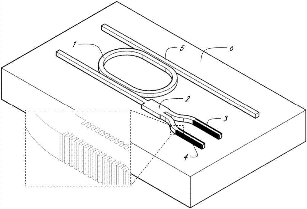
[0022] The overall structure diagram of the optical beat frequency signal transmitting chip of the present invention is as follows figure 1 As shown, it includes a microring laser 1, a multimode interference coupler 2, a static distributed feedback laser 3, a dynamically modulated distributed feedback laser 4, an output directional coupler, an output waveguide 5, and a semiconductor wafer 6; Both the static distributed feedb...


PUM


Abstract

The invention relates to an optical beat signal emitting chip. The optical beat signal emitting chip comprises a micro-ring laser, a multimode interference coupler, a static distributed feedback laser, a dynamic modulation distributed feedback laser, an output directional coupler and output waveguide, and a semiconductor wafer. An injection current of an on-chip device can be adjusted separately due to increase of a common ground electrode on the back of the chip. A coplanar metal transmission line is made on the two distributed feedback lasers, so that direct upconversion from an electric signal to an optical signal is finished, and direct modulation and emission of the electric signal are realized. Both the multimode interference coupler and the output directional coupler and output waveguide are connected with the micro-ring laser. The semiconductor wafer is connected with other devices in the optical beat signal emitting chip. The optical beat signal emitting chip outputs a low-noise beat signal by using physical mechanisms like optical frequency mixing, side mode injection locking and an optical feedback loop.

Description

technical field [0001] The invention relates to a high-speed semiconductor optoelectronic device in the communication field, in particular to an optical beat frequency signal transmitting chip and a preparation method thereof. Background technique [0002] With the progress of the times, people have higher and higher requirements for communication bandwidth and speed. The introduction of optical wireless communication technology can well combine the advantages of bandwidth, high-speed, long-distance optical fiber communication and convenient short-distance wireless communication. It is also possible to greatly reduce the cost of the communication system by centralizing complex communication equipment. In the existing technology, the core idea of ​​wireless communication over optical technology is to use the existing wireless technology in the cellular network, while the communication between the base station and the central office uses optical fiber communication, and the wi...

Claims


Application Information

Patent Timeline
Patent Type & Authority Applications(China)
IPC IPC(8): H04B10/50H04B10/516H01S5/22H01S5/34
CPCH01S5/22H01S5/34H04B10/503H04B10/5059H04B10/516
Inventor 陈钰杰王易余思远蔡鑫伦
Owner SUN YAT SEN UNIV
Learn More