Common-optical path self-calibrating thin film thickness measuring device and measuring method

A film thickness and measuring device technology, applied in measuring devices, optical devices, instruments, etc., can solve the problems of thin film surface morphology damage, difficult demodulation, etc., to improve absolute accuracy, test stability, and large dynamic range. , to achieve the effect of self-calibration

Active Publication Date: 2017-09-15
HEFEI XINWEI INSTR
View PDF10 Cites 12 Cited by
  • Summary
  • Abstract
  • Description
  • Claims
  • Application Information

AI Technical Summary

Problems solved by technology

[0004] In 2013, Ma Xizhi and others from Nanjing University of Aeronautics and Astronautics disclosed an ultrasonic film thickness measuring instrument and its measurement method (Chinese patent application number: 201310198294.9). Measure the correlation characteristics of the reflected pulse to measure the thickness of the oil film; however, this method is only suitable for the measurement of the liquid mode, and different models need to be established for films with different thickness ranges, and the demodulation is difficult
In 2014, Jia Chuanwu of Shandong University and others disclosed a system for measuring film thickness by wide-spectrum optical interferometry (Chinese patent application number: 201410290494.1). Interferometer, the thickness of the film to be tested can be obtained by measuring the length of the Fabry Perot cavity before and after placing the film to be tested under the mirror. This method has a simple structure and high measurement accuracy. Under the mirror, it is easy to damage the morphology of the film surface

Method used


Image

  • Common-optical path self-calibrating thin film thickness measuring device and measuring method
  • Common-optical path self-calibrating thin film thickness measuring device and measuring method
  • Common-optical path self-calibrating thin film thickness measuring device and measuring method

Examples


Embodiment Construction

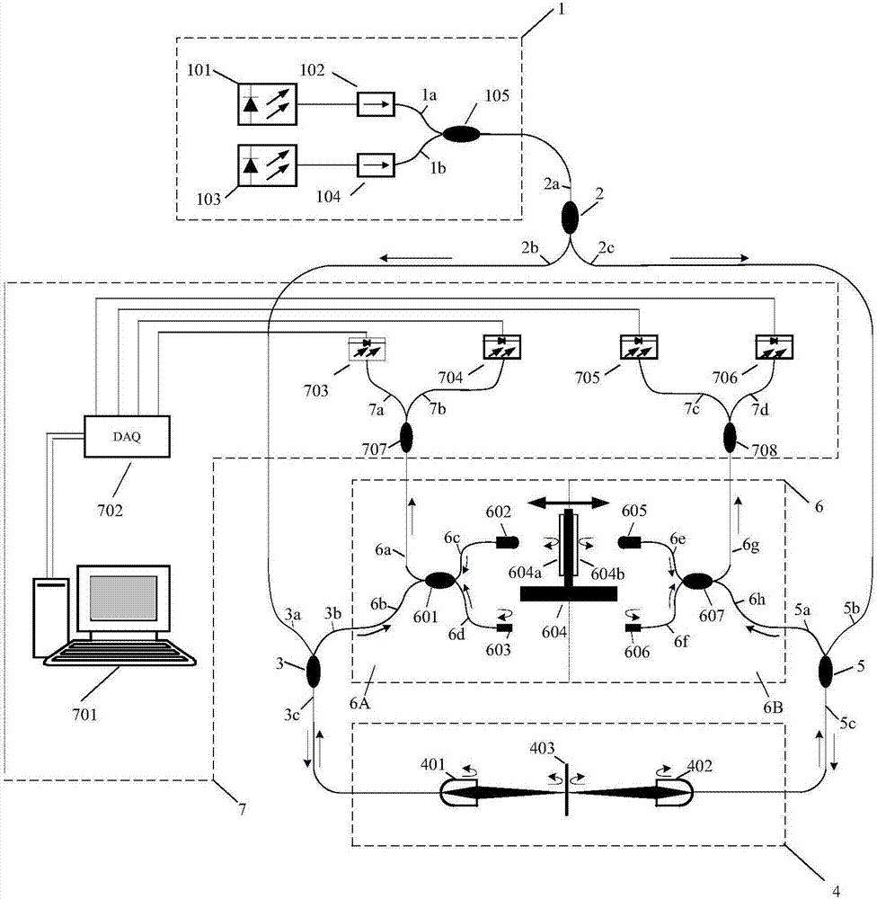
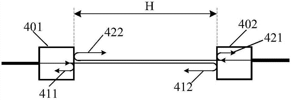
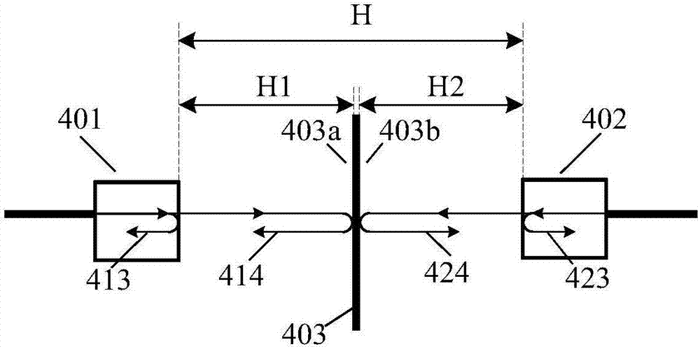
[0030] The common optical path self-calibration film thickness measurement device of the present invention is composed of four parts: a light source output module 1 , a film thickness measurement probe module 4 , an interference and demodulation module 6 , and an acquisition and control module 7 . The components of each module are: (1) The light source output module 1 is composed of a wide-spectrum light source 101, a first isolator 102, a narrowband frequency-stabilized laser light source 103, a second isolator 104, and a first wavelength division multiplexer 105; 2) The film thickness measuring probe module 4 is composed of the first measuring probe 401 and the second measuring probe 402; (3) the interference and demodulation module 6 is composed of the first demodulating interferometer coupler 601, the first collimating mirror 602, The first Faraday mirror 603, the position scanning device 604, the forward movable optical mirror 604a, the reverse movable optical mirror 604b,...


PUM


Abstract

The present invention provides a common-optical path self-calibrating thin film thickness measuring device and measuring method. The measuring device includes a light source output module, a film thickness measurement probe module, an interference and demodulation module and an acquisition and control module; the measuring probes of the measuring device of the invention can simultaneously realize the transmission and reflection of transmitted light, the measurement of an absolute distance H between the two probes can be realized when no thin films to be measured exist; when a thin film to be measured is arranged between the two probes; an absolute distance H1 between one probe and the front surface of the thin film to be measured and an absolute distance H2 between the other probe and the rear surface of the thin film to be measured can be realized; and the thickness of the thin film to be measured can be determined according to an equation that d=H-(H1+H2). With the common-optical path self-calibrating thin film thickness measuring device and measuring method of the invention adopted, the measurement of the thickness of a transparent thin film and an opaque thin film can be realized without calibrating samples required; and since interference light beams share one optical path, influences brought by mechanical instability in a measurement system and the change of an external environment during a measurement process can be eliminated. The common-optical path self-calibrating thin film thickness measuring device and measuring method have the advantages of self-calibration, traceable measuring results, high stability and the like.

Description

technical field [0001] The invention relates to an optical measuring device, in particular to a film thickness measuring device. Specifically, it is a common optical path self-calibration film thickness measuring device. Background technique [0002] With the vigorous development of material science and technology, in order to meet the urgent needs of microelectronics, optoelectronics, new energy and other fields, thin films are used in optical engineering, mechanical engineering, communication engineering, biological engineering, aerospace engineering, chemical engineering, medical engineering and other fields. widely used. One of the core and key parameters of thin film materials is thickness, which not only plays a key role in the preparation of thin films, but also basically determines the mechanical, electromagnetic, photoelectric and optical properties of thin films. [0003] In 1961, N. Schwartz and others proposed a contact probe method that uses high-precision mec...

Claims


Application Information

Patent Timeline
IPC IPC(8): G01B11/06G01B11/02
Inventor 苑勇贵卢旭杨军彭峰李寒阳卢东川祝海波苑立波
Owner HEFEI XINWEI INSTR
Why Eureka
Try Eureka