Pixel circuit and driving method of pixel circuit

A pixel circuit and transistor technology, applied in static indicators, instruments, etc., can solve the problems of inconsistency in the writing of the screen signal of the display screen, narrowing of the line width of the pixel circuit planning diagram, and uneven voltage threshold of the pixel circuit, etc., to achieve Conducive to layout, simple circuit layout, uniform display effect

Active Publication Date: 2019-01-18
JITRI INST OF ORGANIC OPTOELECTRONICS CO LTD
View PDF8 Cites 0 Cited by
  • Summary
  • Abstract
  • Description
  • Claims
  • Application Information

AI Technical Summary

Problems solved by technology

The current mainstream LTPS process, due to the defects of the process itself, causes the problem of uneven voltage threshold (Vth) in the pixel circuit, so the pixel circuit mainly compensates for Vth. For high PPI products (such as microdisplays), due to the pixel layout space Smaller, resulting in the narrowing of the line width of the pixel circuit layout, resulting in an increase in the voltage drop of the power supply voltage, resulting in inconsistent writing of the screen signal of the display screen, resulting in uneven display

Method used


Image

  • Pixel circuit and driving method of pixel circuit
  • Pixel circuit and driving method of pixel circuit
  • Pixel circuit and driving method of pixel circuit

Examples


no. 1 example

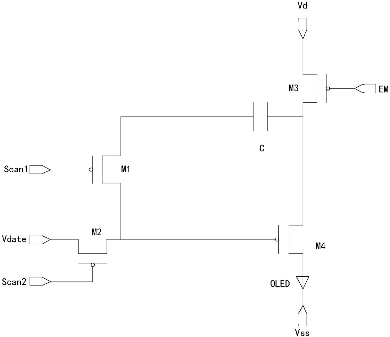
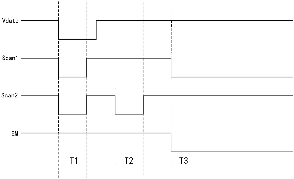
[0031] An embodiment of the present invention provides a pixel circuit, such as figure 1 As shown, the pixel circuit includes a first transistor M1, a second transistor M2, a third transistor M3, a fourth transistor M4, a first scanning signal line Scan1, a second scanning signal line Scan2, a data signal line Vdate, a control signal line EM, capacitor C, power supply and light emitting diode OLED.

[0032] In this embodiment, the gate of the first transistor M1 is connected to the first scanning signal line Scan1, the source of the first transistor M1 is electrically connected to the first plate of the capacitor C, and the first transistor The drain of M1 is connected to the source of the second transistor M2.

[0033] In one embodiment, as image 3 Said, the first transistor M1 may be a double-gate transistor, and the double gates of the first transistor M1 are both connected to the first scanning signal line Scan1. The leakage current can be effectively reduced by using ...

no. 2 example

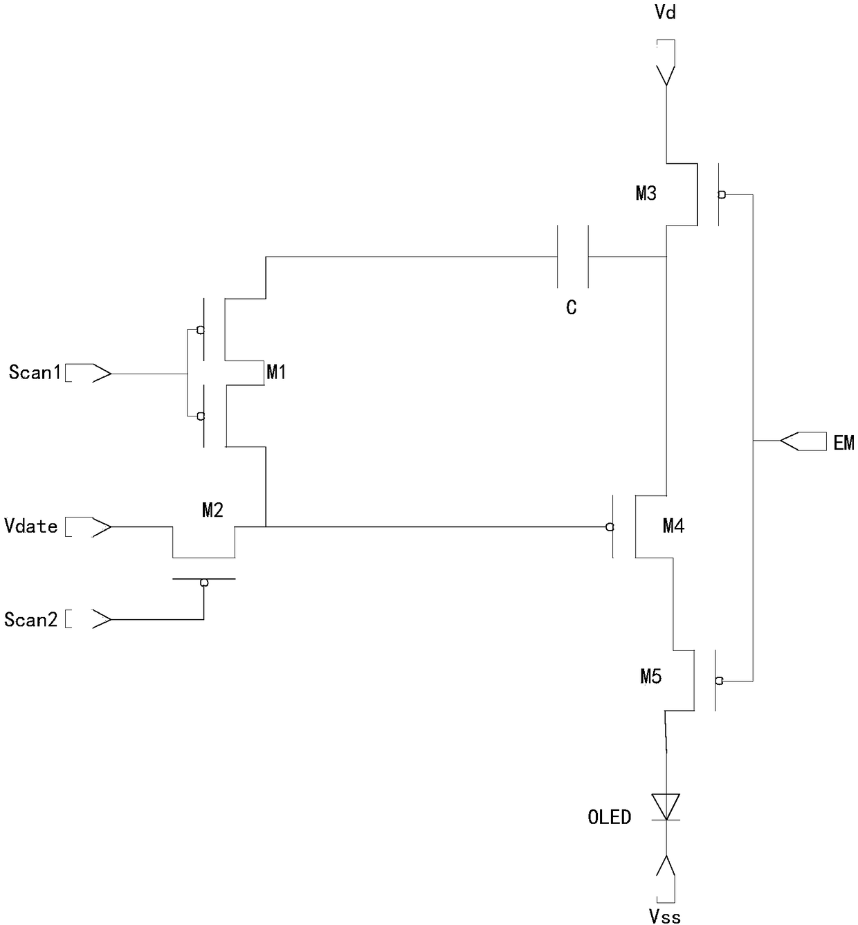
[0056] This embodiment provides a pixel circuit. This embodiment is similar to the first embodiment, and the difference is that the pixel circuit in this embodiment has a fifth transistor M5 added to the pixel circuit in the first embodiment. Specific as image 3 As shown, the pixel circuit further includes a fifth transistor M5.

[0057] In this embodiment, the fifth transistor M5 is connected between the fourth transistor M4 and the light emitting diode OLED, and the source of the fifth transistor M5 is connected to the drain of the fourth transistor M4, so The drain of the fifth transistor M5 is grounded, and the gate of the fifth transistor M5 is connected to the control signal line EM; the control signal line EM sends a control signal to the gate of the fifth transistor M5 to control The fifth transistor M5 is turned on or off.

[0058] For other details in this embodiment, reference may be made to the description in the first embodiment, which will not be repeated here...

no. 3 example

[0061] This embodiment provides a pixel circuit. This embodiment is similar to the first embodiment. The difference is that the pixel circuit in this embodiment has a sixth transistor M6 and a reference voltage flat signal line. For details, please refer to Figure 5 , the pixel circuit further includes a sixth transistor M6 and a reference level signal line.

[0062] In this embodiment, the gate of the sixth transistor M6 is connected to the first scanning signal line Scan1, and the drain of the sixth transistor M6 is connected to the light-emitting diode OLED; the first scanning signal line Scan1 sends A control signal is sent to the gate of the sixth transistor M6 to control the sixth transistor M6 to be turned on or off.

[0063] The reference level signal line is connected to the source of the sixth transistor M6, and the reference level signal line is used to provide an initial current to flow into the light emitting diode OLED through the sixth transistor M6 to initia...


PUM


Abstract

Embodiments of the present invention provide a pixel circuit and a driving method for the pixel circuit. In one embodiment, the pixel circuit includes a first transistor, a second transistor, a third transistor, a fourth transistor, a first scanning signal line, a second scanning signal line, a data signal line, a control signal line, a capacitor, a power supply and LEDs. The source of the first transistor is connected to the first plate of the capacitor, the drain of the first transistor is connected to the source of the second transistor; the second plate of the capacitor is connected to the third transistor The drain of the second transistor is connected to the gate of the fourth transistor, and the source of the second transistor is connected to the data signal line; the source of the third transistor is connected to the power supply connected, the drain of the third transistor is connected to the source of the fourth transistor; the drain of the fourth transistor is connected to the light emitting diode; the cathode of the light emitting diode is grounded.

Description

technical field [0001] The present invention relates to the technical field of driving pixels of displays, in particular to a pixel circuit and a method for driving the pixel circuit. Background technique [0002] AMOLED display technology is gradually replacing traditional display technology (such as liquid crystal display) due to its advantages such as wide color gamut, wide viewing angle, high contrast ratio, and low power consumption. In the AMOLED display screen, the pixel circuit, as a signal control circuit of the pixel point, plays an important role in the display panel. The current mainstream LTPS process, due to the defects of the process itself, causes the problem of uneven voltage threshold (Vth) in the pixel circuit, so the pixel circuit mainly compensates for Vth. For high PPI products (such as microdisplays), due to the pixel layout space Smaller, the line width of the pixel circuit layout is narrowed, the voltage drop of the power supply voltage is increased...

Claims


Application Information

Patent Timeline
Patent Type & Authority Patents(China)
IPC IPC(8): G09G3/3266G09G3/3233
CPCG09G3/3233G09G3/3266G09G2300/0819G09G2300/0861G09G2300/0842G09G3/3291
Inventor 韩媛媛曹朝干祝晓钊王龙冯敏强廖良生
Owner JITRI INST OF ORGANIC OPTOELECTRONICS CO LTD
Why Eureka
Try Eureka