Coated chip dimension packaging structure and packaging method thereof

A chip size packaging and packaging method technology, applied in electrical components, electrical solid devices, circuits, etc., can solve the problems of unprotected sidewalls, chip offset lithography, chip corner stress, etc., to enhance bonding force, improve Yield, effect of enhancing stress rupture strength

Active Publication Date: 2017-09-29
JIANGYIN CHANGDIAN ADVANCED PACKAGING CO LTD
View PDF4 Cites 10 Cited by
  • Summary
  • Abstract
  • Description
  • Claims
  • Application Information

AI Technical Summary

Problems solved by technology

However, wafer-level chip size packaging also faces some problems. As the chip becomes smaller and thinner, and its side wall is not protected, the pick-and-place of the chip during SMT will cause edge stress and even chip fragmentation.
[0003] At the same time, in the traditional fan-out chip size packaging process, the reconstituted wafer is then subjected to the RDL process, which often has the problem of lithography offset caused by chip offset.

Method used


Image

  • Coated chip dimension packaging structure and packaging method thereof
  • Coated chip dimension packaging structure and packaging method thereof
  • Coated chip dimension packaging structure and packaging method thereof

Examples


Embodiment

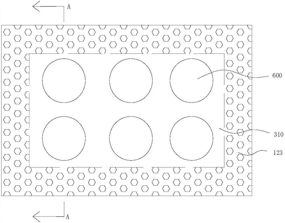
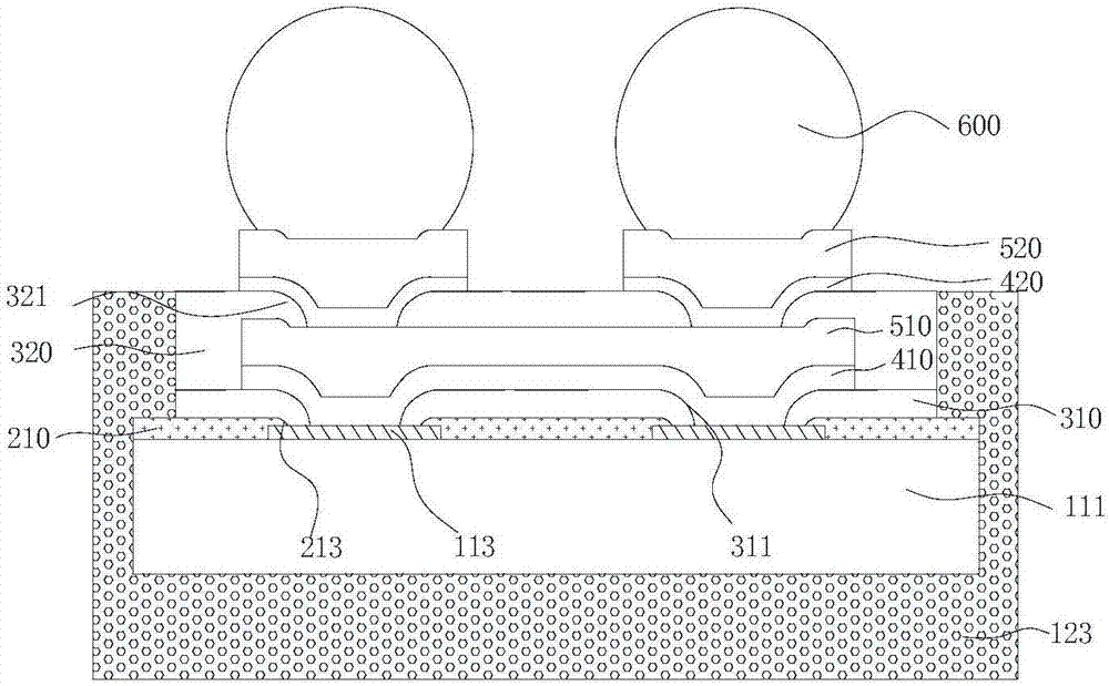
[0061] figure 1 It is a schematic front view of an embodiment of a wrap-around chip-scale packaging structure of the present invention, figure 2 Its A-A sectional schematic diagram.

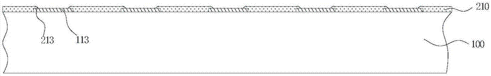
[0062] The present invention is an encapsulation type chip size packaging structure, in which a passivation layer 210 is provided on the front side of the silicon base body 111 and a passivation layer opening 213 is opened, the chip electrode 113 is embedded in the front side of the silicon base body 111 from the back side, and the passivation layer opening 213 exposes the front surface of the chip electrode 113 .

[0063]The upper surface of the passivation layer 210 is provided with a dielectric layer I310 and an opening I311 of the dielectric layer I is provided. The opening I311 of the dielectric layer I exposes the front surface of the chip electrode 113, and the dielectric layer I310 does not cover the edge of the passivation layer 210. The metal seed layer I 410 , the metal layer I 510 ...


PUM


Abstract

The present invention discloses a coated chip dimension packaging structure and a packaging method thereof, belonging to the semiconductor packaging technology field. A passivation layer (210) is arranged at the right surface of a silicon-based body (111), a chip electrode (113) is embedded into the right side of the silicon-based body (111) from the back, the upper surface of the passivation layer (210) is provided with a dielectric layer I (310), the edge of the passivation layer (210) is not coated with the dielectric layer I (310), the passivation layer (210) is coated with a metal seed layer I (410), a metal layer I (510) and a dielectric layer II (320), and the dielectric layer II (320) is provided with a dielectric layer II opening I (321) exposed out of the upper surface of a metal layer I (510); and the upper surface of the metal layer I (510) is provided with a bump bottom metal II, an encapsulated layer II (123) is arranged around the silicon-based body (111) and at the back surface of the silicon-based body (111), and the encapsulated layer II (123) is extended upwards to wrap the exposure portion of the passivation layer (210) so as to realize that insulation protection side walls can be performed and the leakage or short circuit is not easy so as to avoid photoetching offset caused by chip offset.

Description

technical field [0001] The invention relates to an encapsulating chip size packaging structure and a packaging method thereof, belonging to the technical field of semiconductor packaging. Background technique [0002] With the increase of wireless handheld devices, palmtop computers and other mobile electronic devices, consumers' demand for various products with small appearance and rich features is also increasing day by day. , miniaturization and low cost" development trend brings challenges and opportunities. Wafer-level chip size packaging technology meets the requirements of electronic products for smaller, more functional, and higher reliability circuit components. However, wafer-level chip size packaging also faces some problems. As the chip becomes smaller and thinner, and its sidewall is not protected, the pick-and-place of the chip during SMT will cause corner stress and even chip fragmentation. [0003] At the same time, in the traditional fan-out chip size pack...

Claims


Application Information

Patent Timeline
Patent Type & Authority Applications(China)
IPC IPC(8): H01L23/31H01L21/56
CPCH01L21/561H01L23/3128H01L2224/96H01L2924/181H01L2224/11H01L2224/16225H01L2224/04105H01L2224/12105H01L2924/00012
Inventor 徐虹张黎陈栋陈锦辉赖志明
Owner JIANGYIN CHANGDIAN ADVANCED PACKAGING CO LTD
Why Eureka
Try Eureka