Silicon-based organic light emitting device of higher performance and manufacturing method thereof

A technology of organic light-emitting devices and organic light-emitting layers, which is applied in the manufacture of semiconductor/solid-state devices, electric solid-state devices, semiconductor devices, etc., can solve problems such as affecting luminous efficiency, unevenness, unevenness and wrinkles on the surface or side of the bottom electrode, and achieves Improve luminous efficiency and improve the effect of flatness

Active Publication Date: 2017-09-29
南京昀光科技有限公司
View PDF8 Cites 0 Cited by
  • Summary
  • Abstract
  • Description
  • Claims
  • Application Information

AI Technical Summary

Problems solved by technology

[0002] In the existing silicon-based organic light-emitting device structure, the bottom electrode is generally a three-layer or five-layer structure, usually a vertical five-layer structure of titanium, titanium nitride, aluminum, titanium, and titanium nitride. For example, the authorized announcement number is This structure is disclosed in "CN102629667B" titled "Silicon-based top-emitting organic light-emitting microdisplay device and its preparation method". Electrode surface or sides are uneven, such as figure 1 shown
In addition, the overall height of the five-layer vertical bottom electrode structure is relatively high. When the organic light-emitting layer is laid on the bottom electrode, it is easy to form unevenness and wrinkles, which will affect the luminous efficiency.

Method used


Image

  • Silicon-based organic light emitting device of higher performance and manufacturing method thereof
  • Silicon-based organic light emitting device of higher performance and manufacturing method thereof
  • Silicon-based organic light emitting device of higher performance and manufacturing method thereof

Examples


no. 1 example

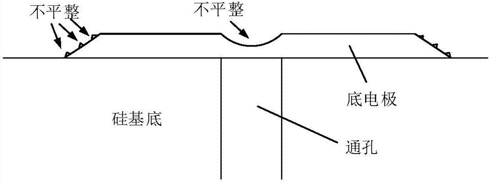
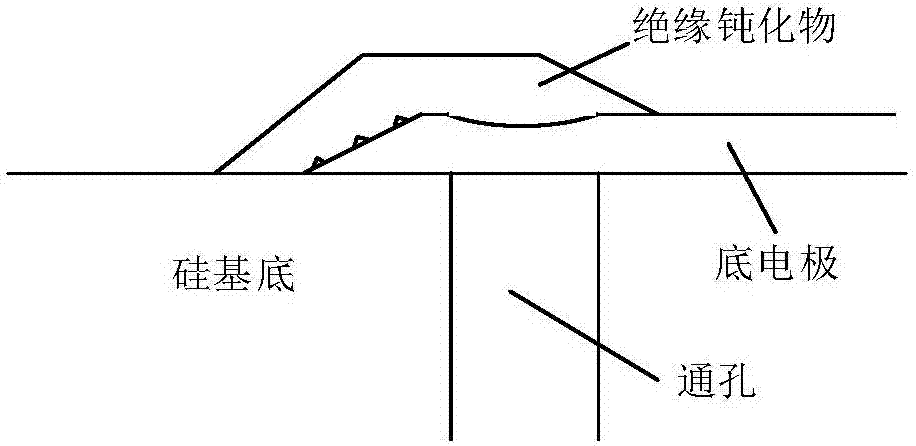
[0040] Such as image 3 As shown, the silicon-based organic light-emitting device described in the present invention includes a silicon substrate 10, a metal-oxide semiconductor field-effect transistor 11, a first metal layer 12, a through hole 13, a bottom electrode 14, an organic light-emitting layer 15, and a top electrode 16 , a thin film encapsulation layer 17 and a common electrode 18, the metal-oxide semiconductor field effect transistor 11 is located in the silicon substrate 10, the bottom electrode 14 protrudes from the silicon substrate surface 10, and the edge of the bottom electrode 14 is formed by The insulating passivation 20 covers and the uncoated area of ​​the bottom electrode 14 is a light emitting area, the common electrode 18 selectively covers the insulating passivation 20, and the through hole 13 connects the first metal layer 12 and The bottom electrode 14 .

[0041] Further, as Figure 4 As shown, the organic light-emitting layer 15 covers the bottom ...

no. 2 example

[0047] In this embodiment, the silicon-based organic light-emitting device is basically the same as the first embodiment, in particular, the top view of the bottom electrode 14 is shown in Figure 7(a)-(c), the through hole 13 is arranged at the edge or four corners of the bottom electrode and protrudes from the light-emitting area 40 , the protruding part is 91 , and the bottom electrode is covered with insulating passivation 20 . Further, the bottom electrode portion on the through hole 13 is covered by the insulating passivation 20 . Figure 7(a) is a top view of the through hole 13 arranged at the edge of the bottom electrode, Figure 7(b) is a top view of the through hole 13 arranged at the corner of the bottom electrode, and Figure 7(c) is another through hole 13 is the top view of the corner position of the bottom electrode.

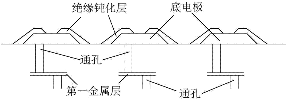
[0048] further, Figure 8 A pixel array composed of several bottom electrodes 14 is illustrated, and in this array, the positions where the throug...

no. 3 example

[0054] In this embodiment, the silicon-based organic light-emitting device is basically the same as the first embodiment, in particular, a second metal layer is provided between the bottom electrode and the first metal layer, and the through hole and the first metal layer are arranged staggered at the same level, such as Figure 11 shown.

[0055] Further, the second metal layer is configured as a ground or a power supply, and the material of the second metal layer includes Al, Ag, Ti, W, Cu, Ta simple substance or one of oxides, nitrides, and silicides. One or a mixture of the above materials in any proportion.

[0056] Further, the thickness of the second metal layer is 50nm-700nm.

[0057] The present invention also provides a method for manufacturing the silicon-based organic light-emitting device, comprising the following steps: making a bottom electrode on a silicon-based substrate; using a mask to directly make an insulating passivation or first making an insulating p...


PUM

PropertyMeasurementUnit
Heightaaaaaaaaaa
Thicknessaaaaaaaaaa

Abstract

The invention discloses a silicon-based organic light emitting device of higher performance and a manufacturing method thereof, relating to the field of silicon-based organic light emitting. The silicon-based organic light emitting device includes a silicon substrate, a metal-oxide semiconductor field effect transistor, a first metal layer, through holes, bottom electrodes, an organic light emitting layer, a top electrode, and a thin film encapsulation layer. The metal-oxide semiconductor field effect transistor is disposed in the silicon substrate. The bottom electrodes protrude from the surface of the silicon substrate, and the edges of the bottom electrodes are covered with insulation inactivator. The organic light emitting layer covers the bottom electrodes and the insulation inactivator. The top electrode covers the organic light emitting layer. The thin film encapsulation layer covers the top electrode. According to the silicon-based organic light emitting device and the manufacturing method thereof, the through holes are shifted, and the edges of the bottom electrodes are wrapped, which greatly improves the laying smoothness of the organic light emitting layer, and increases the luminous efficiency.

Description

technical field [0001] The invention relates to the field of silicon-based organic light-emitting devices, in particular to a silicon-based organic light-emitting device with improved performance and a manufacturing method thereof. Background technique [0002] In the existing silicon-based organic light-emitting device structure, the bottom electrode is generally a three-layer or five-layer structure, usually a vertical five-layer structure of titanium, titanium nitride, aluminum, titanium, and titanium nitride. For example, the authorized announcement number is This structure is disclosed in "CN102629667B" titled "Silicon-based top-emitting organic light-emitting microdisplay device and its preparation method". Electrode surface or sides are uneven, such as figure 1 shown. In addition, the overall height of the five-layer vertical bottom electrode structure is relatively high. When an organic light-emitting layer is laid on the bottom electrode, it is easy to form uneven...

Claims


Application Information

Patent Timeline
IPC IPC(8): H01L51/52H01L27/32H01L51/56
CPCH10K59/12H10K50/856H10K71/00
Inventor 季渊沈伟星
Owner 南京昀光科技有限公司
Why Eureka
Try Eureka