
Fabrication method of GaN high electron mobility transistor (HEMT) device

A manufacturing method and device technology, which is applied in the field of GaNHEMT device manufacturing, can solve the problems of inconspicuousness and high difficulty in realization, achieve the effects of high process compatibility, reduce device current collapse, and increase the number of devices

Active Publication Date: 2017-10-10
CHENGDU HIWAFER SEMICON CO LTD
View PDF3 Cites 5 Cited by
  • Summary
  • Abstract
  • Description
  • Claims
  • Application Information

AI Technical Summary

Problems solved by technology

However, the above method is difficult to realize in the process, and it is not obvious to the

Method used


Image

  • Fabrication method of GaN high electron mobility transistor (HEMT) device
  • Fabrication method of GaN high electron mobility transistor (HEMT) device
  • Fabrication method of GaN high electron mobility transistor (HEMT) device

Examples


Embodiment Construction

[0026] In order to make the purpose, technical solution and advantages of the present application clearer, the present application will be further described in detail below in conjunction with the accompanying drawings and specific embodiments. For simplicity, some technical features known to those skilled in the art are omitted from the following description.

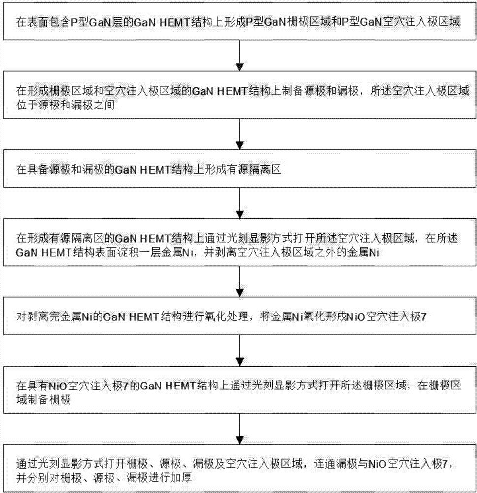
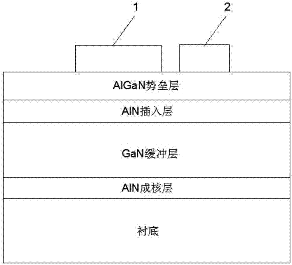
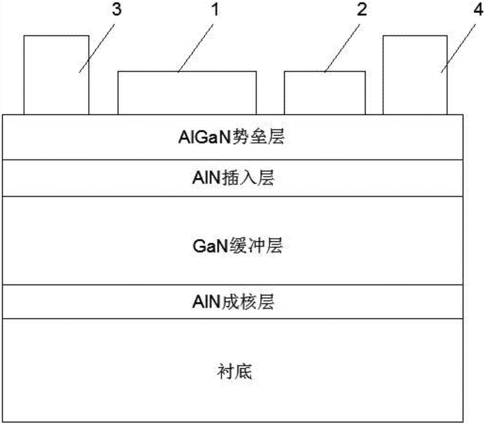
[0027] Such as figure 1 As shown, the GaN HEMT structure of this embodiment includes a substrate, an AlN nucleation layer, a GaN buffer layer, an AlN insertion layer, and an AlGaN barrier layer from bottom to top. There is a P-type GaN layer on the AlGaN barrier layer. The GaN HEMT The manufacturing method of the device includes the following steps:

[0028] S1. Forming a P-type GaN gate region 1 and a P-type GaN hole injector region 2 on a GaN HEMT structure whose surface includes a P-type GaN layer;

[0029] Step S1 is specifically: using AZ5214 photoresist as a protective mask, forming a protective mask for the ga...


PUM


Abstract

The invention relates to the technical field of semiconductor manufacturing, in particular to a fabrication method of a GaN high electron mobility transistor (HEMT) device. The fabrication method comprises the following steps of S1, forming a P-type GaN grid region and a P-type GaN hole injector region on a GaN HEMT structure; S2, preparing source-drain ohmic contact; S3, forming an active isolation region on the GaN HEMT structure; S4, opening the hole injector region by a photoetching and developing mode, depositing metal Ni, and performing stripping; S5, oxidizing the metal Ni to form an NiO hole injector; S6, opening the grid region by the photoetching and developing mode, and preparing a grid on the gird region; and S7, opening the grid, a source, a rain and the hole injector region by the photoetching and developing mode, communicating the drain with the NiO hole injector, and respectively thickening the grid, the source and the drain. According to the fabrication method, the hole injector is additionally arranged between the grid and the drain, holes are injected to a surface of an AlGaN barrier layer to compensate electrons which are trapped, so that depletion of channel two-dimensional electrical gas is reduced, and the current collapse resistant capability of the device is improved.

Description

technical field [0001] The invention belongs to the technical field of semiconductor manufacturing, and in particular relates to a method for manufacturing a GaN HEMT device. Background technique [0002] Because of its wide band gap, GaN materials make GaN HEMT devices based on them have high breakdown voltage, high current density and low on-resistance, and are the core devices of modern power transmission systems. The primary condition for GaN HEMT as a power electronic device is the enhanced working mode. The hotspot in the scientific research and industry circles is the GaN HEMT device with a P-type GaN gate. The specific method is to insert a The P-type GaN layer raises the triangular potential well at the lower AlGaN / GaN heterojunction interface to above the Fermi level through the PN built-in electric field, thereby forming an enhanced channel. With the deepening of research, the P-type GaN gate technology has also encountered a bottleneck. In the above process tec...

Claims


Application Information

Patent Timeline
Patent Type & Authority Applications(China)
IPC IPC(8): H01L21/336
Inventor 林书勋
Owner CHENGDU HIWAFER SEMICON CO LTD
Learn More