Method of fabricating circuit on ductile flexible substrate
A flexible substrate and circuit technology, applied in chemical/electrolytic methods to remove conductive materials, photolithography/patterning, patterning and photolithography, etc., can solve the problem of increasing the circuit manufacturing process and production costs, and reducing the overall extensibility of the circuit , complex polyimide patterning process, etc., to overcome cracks and open circuits, avoid mismatching problems, and reduce equipment dependence
- Summary
- Abstract
- Description
- Claims
- Application Information
AI Technical Summary
Problems solved by technology
Method used
Image

Examples
Embodiment 1
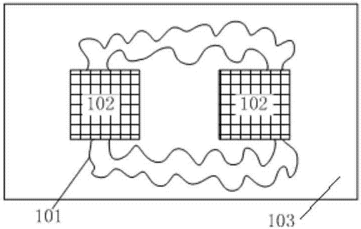
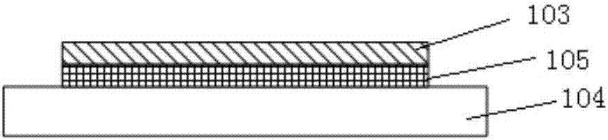
[0036] combine Figure 1 to Figure 8 , the present invention can be applied to the manufacture of flexible electronic devices of various structures, and has no requirements on the material, structure and shape of the circuit. This embodiment is based on the manufacture of polydimethylsiloxane membrane (PDMS) figure 1 The circuit diagram shown is an example to illustrate the implementation method of the present invention. 101 is a circuit interconnection wire, 102 is a circuit function module, and 103 is an extensible flexible substrate of polydimethylsiloxane. In order to adapt to the stretching of the extensible flexible substrate 103, the circuit interconnection wire 101 is in the shape of a curved connection with a width of 0.5 mm.
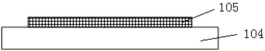
[0037] Step 1: If figure 2 As shown, a clean and dust-free glass plate is selected as the hard thin plate 104, and a small amount of ordinary double-sided adhesive tape is pasted on the surface of the glass plate. Surface, pay attention to...
PUM
| Property | Measurement | Unit |
|---|---|---|
| Thickness | aaaaa | aaaaa |
Abstract
Description
Claims
Application Information
 - R&D
- Intellectual Property
- Life Sciences
- Materials
- Tech Scout
- Unparalleled Data Quality
- Higher Quality Content
- 60% Fewer Hallucinations
Browse by: Latest US Patents, China's latest patents, Technical Efficacy Thesaurus, Application Domain, Technology Topic, Popular Technical Reports.
© 2025 PatSnap. All rights reserved.Legal|Privacy policy|Modern Slavery Act Transparency Statement|Sitemap|About US| Contact US: help@patsnap.com