PCBA asymmetric solder pad steel mesh windowing method and system

A window opening system, asymmetric technology, used in metallurgical bonding, electrical components, printed circuit manufacturing, etc. The effect of improving competitiveness

Active Publication Date: 2017-10-20
ZHENGZHOU YUNHAI INFORMATION TECH CO LTD
View PDF5 Cites 7 Cited by
  • Summary
  • Abstract
  • Description
  • Claims
  • Application Information

AI Technical Summary

Problems solved by technology

[0004] The purpose of the present invention is to provide a PCBA asymmetric pad stencil window opening method, so that when the solder paste melts, the pulling force generated on the electrical co...

Method used


Image

  • PCBA asymmetric solder pad steel mesh windowing method and system
  • PCBA asymmetric solder pad steel mesh windowing method and system
  • PCBA asymmetric solder pad steel mesh windowing method and system

Examples


Embodiment Construction

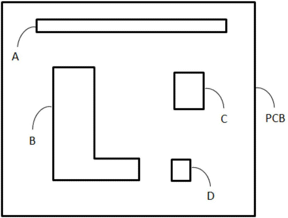
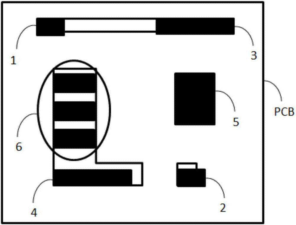
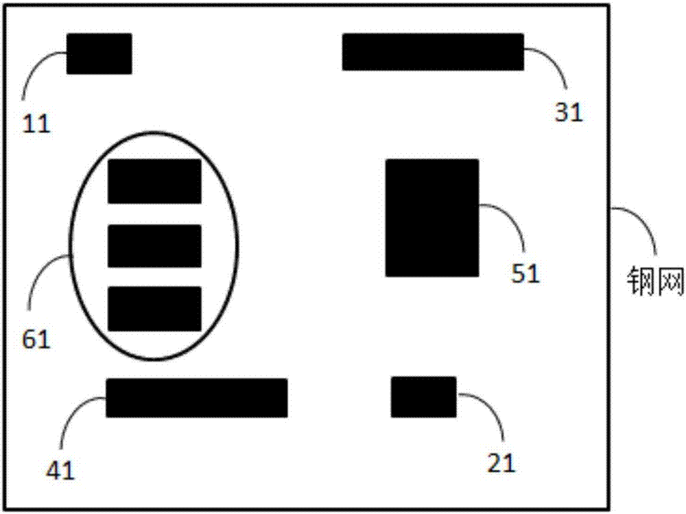
[0029] In order to clearly illustrate the technical features of the present solution, the present invention will be described in detail below through specific implementation methods and in conjunction with the accompanying drawings. The following disclosure provides many different embodiments or examples for implementing different structures of the present invention. To simplify the disclosure of the present invention, components and arrangements of specific examples are described below. Furthermore, the present invention may repeat reference numerals and / or letters in different instances. This repetition is for the purpose of simplicity and clarity and does not in itself indicate a relationship between the various embodiments and / or arrangements discussed. It should be noted that components illustrated in the figures are not necessarily drawn to scale. Descriptions of well-known components and processing techniques and processes are omitted herein to avoid unnecessarily lim...


PUM

PropertyMeasurementUnit
Thicknessaaaaaaaaaa

Abstract

The invention provides a PCBA asymmetric solder pad steel mesh windowing method and system. The method comprises the following steps that the actual tin soldering area of a solder pad is determined, and the area of the diagonal direction of the tin soldering area is identical and the area of the left and right sides is identical; the corresponding steel mesh thickness of the solder pad is determined; and cutting and windowing are performed according to the corresponding position of the actual tin soldering area of the solder pad in the steel mesh. The diagonal area of windowing of the steel mesh is set to be identical and the left and right area is set to be identical, and the tin paste volume of the position of the identical area is the same in performing tin paste printing so that the pull force for the electrical element pins of the identical area position is the same, the problems of poor quality of deviation, inclination and floating can be effectively solved, the yield rate of circuit board production can be greatly enhanced, the production cost can be reduced and the circuit board competitiveness can be enhanced.

Description

technical field [0001] The invention relates to the field of circuit board processing and production, in particular to a method for opening a window of a PCBA asymmetric pad steel mesh. Background technique [0002] With the rapid development of today's electronics industry, almost all electronic equipment needs the support of PCBA (assembly of PCB), that is, the electronic devices are assembled on the circuit board through the surface packaging process, and then the assembled PCB is assembled with the casing to form a finished product. The basic requirements for PCBA assembly are consistency and correctness, and differences must be controlled, and variations are not allowed. [0003] Today, the electrical components on PCBA are rapidly developing toward high integration and miniaturization, and the design of PCBA also tends to be miniaturized. Smaller devices and smaller spacing can easily cause asymmetric distribution of electrical component pins, resulting in The distrib...

Claims


Application Information

Patent Timeline
IPC IPC(8): H05K3/34
CPCH05K3/341H05K2203/04
Inventor 蒋海华
Owner ZHENGZHOU YUNHAI INFORMATION TECH CO LTD
Why Eureka
Try Eureka