FPGA logic testing structure and method

A logic test and logic technology, applied in the field of FPGA logic test, can solve the problems of not being able to quickly locate the problem, occupying logic resources, unfavorable debugging, etc., and achieve the effects of easy promotion, wide application range, and low resource occupation

Inactive Publication Date: 2017-10-24
JINAN INSPUR HIGH TECH TECH DEV CO LTD
View PDF5 Cites 8 Cited by
  • Summary
  • Abstract
  • Description
  • Claims
  • Application Information

AI Technical Summary

Problems solved by technology

[0003] In the development process, it is necessary to test and verify the circuit logic function described by the hardware description language. Generally, the on-chip logic analysis function provided by the FPGA manufacturer can be used, or the logic test and verification can be carried out by using a dedicated logic

Method used


Image

  • FPGA logic testing structure and method

Examples


Embodiment Construction

[0029] In order to enable those skilled in the art to better understand the solutions of the present invention, the present invention will be further described in detail below in conjunction with specific embodiments. Apparently, the described embodiments are only some of the embodiments of the present invention, but not all of them. Based on the embodiments of the present invention, all other embodiments obtained by persons of ordinary skill in the art without making creative efforts belong to the protection scope of the present invention.

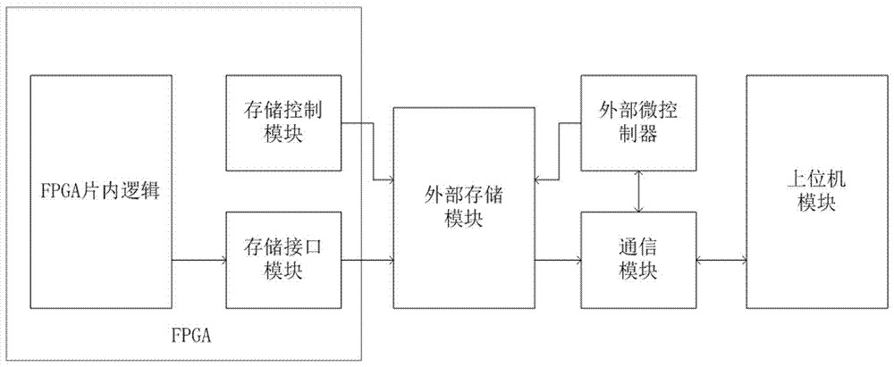
[0030] as attached figure 1 As shown, a FPGA logic test structure includes,

[0031] The FPGA module provides signals or variables to be tested within the FPGA;

[0032] An external storage module is connected to the FPGA module and stores and processes the internal signal to be measured or the variable from the FPGA module;

[0033] The control module is connected to the external storage module, and selects the stored signal or variab...


PUM


Abstract

The invention discloses an FPGA logic testing structure and method. The FPGA logic testing structure includes an FPGA module, an external storage module and a control module, wherein the FPGA module provides internal signals to be tested or variables of the FPGA; the external storage module is connected with the FPGA module and performs storage processing on the internal signals to be tested or variables of the FPGA module; and the control module is connected with the external storage module, selects the stored signals to be tested or variables, completes external reading, determines the internal logic running state of the FPGA module and then displays the internal logic running state of the FPGA module. Compared with the prior art, the FPGA logic testing structure and method can conveniently and efficiently track and observe the signals to be tested, can verify internal logic of FPGA, can greatly improve the efficiency of the initial stage and debugging stage of the project, are low in occupancy of resources, can reduce the development cost relative to a special instrument, have high practicability, are wide in the application range, and are easy for popularization.

Description

technical field [0001] The invention relates to the technical field of FPGA logic testing, in particular to an FPGA logic testing structure and method capable of rapidly locating problems. Background technique [0002] FPGA (Field Programmable Gate Array) is a semiconductor IC that completes circuit design with hardware description language (Verilog or VHDL). After simple synthesis and layout, it is quickly burned to FPGA for testing and can be used for various functional digital Circuit development can also be used for modern IC design verification. [0003] In the development process, it is necessary to test and verify the circuit logic function described by the hardware description language. Generally, the on-chip logic analysis function provided by the FPGA manufacturer can be used, or the logic test and verification can be carried out by using a dedicated logic analysis instrument. However, these methods may take up An uncertain amount of FPGA internal logic resources ...

Claims


Application Information

Patent Timeline
IPC IPC(8): G01R31/3177
CPCG01R31/3177
Inventor 王子彤姜凯聂林川
Owner JINAN INSPUR HIGH TECH TECH DEV CO LTD
Why Eureka
Try Eureka