Non-doped white light luminous layer series organic light-emitting device

An electroluminescent device, non-doped technology, applied in electric solid devices, electrical components, semiconductor devices, etc., can solve the problems of unfavorable device spectral stability, high color rendering index, complex structure, etc., to improve production repeatability and Production efficiency, simplification of the production process, and the effect of facilitating commercialization

Inactive Publication Date: 2017-10-27
GUANGDONG UNIV OF TECH
View PDF4 Cites 2 Cited by
  • Summary
  • Abstract
  • Description
  • Claims
  • Application Information

AI Technical Summary

Problems solved by technology

[0004] At present, the structure of white light tandem devices in the literature is complex, and doping technology is required to prepare the light-emitting layer; in addition, there is generally only one light color in a light-emitting unit, which is not conducive to the spectral stability and high color rendering index of the device.

Method used


Image

  • Non-doped white light luminous layer series organic light-emitting device
  • Non-doped white light luminous layer series organic light-emitting device
  • Non-doped white light luminous layer series organic light-emitting device

Examples


Embodiment 1

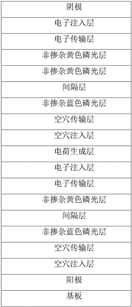
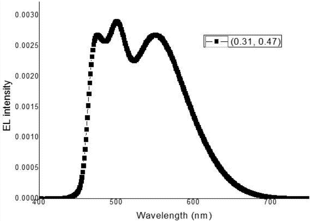
[0029] Such as Figure 1-2 As shown, a non-doped white light emitting layer is connected in series with an organic electroluminescent device. The structure of the device is: ITO / HAT-CN(100nm) / NPB(15nm) / TCTA(5nm) / FIrpic(0.2nm) / TCTA (1nm)Ir(dmppy) 2 (dpp)(0.9nm) / Bepp 2 (15nm) / Bepp 2 :KBH 4 (10nm, 15%) / HAT-CN(120nm) / NPB(15nm) / TCTA(5nm) / FIrpic(0.2nm) / TCTA(1nm)Ir(dmppy) 2 (dpp)(0.9nm) / TmPyPB(50nm) / Cs 2 CO 3 (1nm) / Al(200nm).

[0030] The structure of the device is sequentially superimposed by the following functional layers:

[0031] Substrate, anode, hole injection layer, hole transport layer, undoped blue phosphor layer, spacer layer, undoped yellow phosphor layer, electron transport layer, electron injection layer, charge generation layer, hole injection layer, void Hole transport layer, undoped blue phosphorescent layer, spacer layer, undoped yellow phosphorescent layer, undoped yellow phosphorescent layer, electron transport layer, electron injection layer, cathode.

[0032] The abo...

Embodiment 2

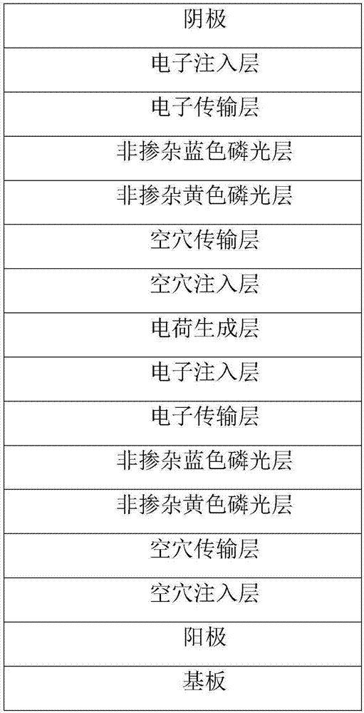
[0070] Such as image 3 As shown, a non-doped white light emitting layer is connected in series with an organic electroluminescent device. The device includes a substrate, an anode, a hole injection layer, a hole transport layer, a non-doped yellow phosphorescent layer, and a non-doped blue from bottom to top. Color phosphorescent layer, electron transport layer, electron injection layer, charge generation layer, hole injection layer, hole transport layer, non-doped yellow phosphor layer, non-doped blue phosphor layer, electron transport layer, electron injection layer and cathode .

[0071] The above-mentioned substrate is glass.

[0072] The above-mentioned anode is an ITO film.

[0073] The above hole injection layer is a 100 nm thick HAT-CN thin film.

[0074] The above hole transport layer includes a first hole transport layer and a second hole transport layer stacked in sequence, the first hole transport layer is a 10nm thick NPB film, and the second hole transport layer is a 1...

Embodiment 3

[0087] Such as Figure 4 As shown, a non-doped white light emitting layer is connected in series with an organic electroluminescent device. The device includes a substrate, an anode, a hole injection layer, a hole transport layer, a non-doped yellow phosphorescent layer, a spacer layer, and a non-doped yellow phosphor layer from bottom to top. Doped blue phosphor layer, electron transport layer, electron injection layer, charge generation layer, hole injection layer, hole transport layer, undoped yellow phosphor layer, spacer layer, undoped blue phosphor layer, electron transport layer , Electron injection layer and cathode.

[0088] The above-mentioned substrate is glass.

[0089] The above-mentioned anode is an ITO film.

[0090] The above hole injection layer is a 100 nm thick HAT-CN thin film.

[0091] The above-mentioned hole transport layer includes a first hole transport layer and a second hole transport layer stacked in sequence, the first hole transport layer is a 10 nm thic...


PUM


Abstract

The present invention discloses a non-doped white light luminous layer series organic light-emitting device. The device comprises, from bottom to top, a substrate, an anode, a hole injection layer, a hole transport layer, a luminous layer, an electron transport layer, an electron injection layer, a charge generation layer, a hole injection layer, a hole transport layer, a luminous layer, an electron transport layer, an electron injection layer and a cathode, wherein the luminous layers are one or more of a non-doped yellow phosphor layer, a non-doped blue phosphor layer, a non-doped red phosphor layer and a non-doped green phosphor layer; a spacer layer is arranged between the luminous layers; and the thickness of the luminous layer is in a range of 0.01 to 200nm, the thickness of the luminous layer is in a range of 0.01 to 100nm, and the thickness of the spacer layer is in a range of 0.1 to 30nm. The non-doped white light luminous layer series organic light-emitting device has a simple structure and a simple process, is stable in spectrum, and has the advantages of simple and convenient process, low cost and the like, and usage of any doping technologies is not involved in the luminous layers.

Description

Technical field [0001] The invention relates to the technical field of organic semiconductors, in particular to an organic electroluminescence device with non-doped white light emitting layers connected in series. Background technique [0002] OLED (English full name Organic Light Emitting Diodes, meaning organic electroluminescent device, referred to as OLED) has autonomous light emission, wide viewing angle, light weight, wide temperature adaptation range, large area, full curing, flexibility, low power consumption, and response Many advantages, such as fast speed and low manufacturing cost, have important applications in the display and lighting fields, and thus have received extensive attention from academia and industry. [0003] In order to further improve the efficiency and life of the device, the researchers stacked multiple independent light-emitting units, so that the same size of current flows through multiple different light-emitting units to emit light together to impr...

Claims


Application Information

Patent Timeline
Patent Type & Authority Applications(China)
IPC IPC(8): H01L51/50H01L51/52
CPCH10K30/865H10K50/15H10K50/16H10K50/86H10K50/11
Inventor 罗向东刘佰全杨炎锋黄林轶杨亿斌
Owner GUANGDONG UNIV OF TECH
Why Eureka
Try Eureka