Microfluidic chip for detecting tumor markers based on uniformly distributed microspheres, and use method thereof

A microfluidic chip, tumor marker technology, applied in the field of biosensors, can solve problems such as obstruction of liquid flow, complicated experimental steps, unfavorable analysis, etc., to prevent clogging, simplify experimental operations, and avoid the effects of fluorescent signal interference.

Active Publication Date: 2017-11-07
SHANGHAI INST OF MICROSYSTEM & INFORMATION TECH CHINESE ACAD OF SCI
5 Cites 7 Cited by

AI-Extracted Technical Summary

Problems solved by technology

The method of driving or trapping microspheres with special properties by using magnetic or electric fields often requires equipment to generate external fields, which complicates the experimental steps
However, in the method of hydrodynamic interception, if the structure is not properly designed, the microspheres will often accumulat...

Method used

(2) photoresist is spin-coated on the silicon chip after cleaning, thickness is 3 μ m, through a series of photolithography processes such as exposure, development, the photoresist on silicon chip is carried out according to the pattern of mask plate patterned. Using the photoresist pattern after photolithography as a mask, ...

Abstract

The invention relates to a microfluidic chip for detecting tumor markers based on uniformly distributed microspheres, and a use method thereof. The microfluidic chip comprises a sample inlet, a sample outlet and a plurality of micro-column arrays parallel to a liquid flowing direction, wherein the gaps between the micro-column arrays are main flowing channels, and the narrowest gap between the adjacent micro-columns in the micro-column arrays is slightly smaller than the diameter of the microsphere. According to the present invention, based on the principle of fluid diffusion, the structure is simple, the complex flow resistance theoretical calculation is not required, the microspheres can be uniformly arranged between the gaps of the micro-columns, and the interference of the fluorescence signals can be avoided with the discretely distributed microspheres; the microspheres can be combined with different antibodies according to the requirements so as to detect different markers; and the sample injection time can be shortened through the used incubation method, the sample injection and the washing are integrated so as to simplify the experiment operation, and the microfluidic chip can be used for the biochemical detection using the microspheres as the carrier, and has the good application prospects.

Application Domain

Technology Topic

Image

  • Microfluidic chip for detecting tumor markers based on uniformly distributed microspheres, and use method thereof
  • Microfluidic chip for detecting tumor markers based on uniformly distributed microspheres, and use method thereof
  • Microfluidic chip for detecting tumor markers based on uniformly distributed microspheres, and use method thereof

Examples

  • Experimental program(1)

Example Embodiment

[0019] Example 1
[0020] 1. Preparation of microfluidic chip
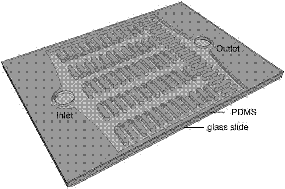
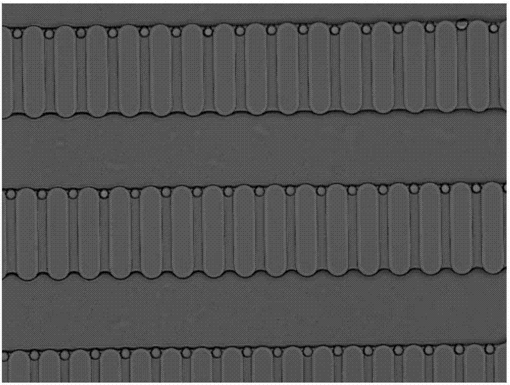
[0021] (1) Use CAD software to make the required mask. The length of the micro-pillars is 130 μm, the width is 30 μm, the narrowest spacing between the micro-pillars is 13 μm, the distance between the micro-pillar array is 100 μm, and the entire chip is about 25 μm. A micro-pillar array, each array has about 200 micro-pillars, the length of the micro-pillars is perpendicular to the main flow direction.
[0022] (2) The photoresist is spin-coated on the cleaned silicon wafer with a thickness of 3 μm. After a series of photolithography processes such as exposure and development, the photoresist on the silicon wafer is patterned according to the pattern of the mask. Using the photoresist pattern after photolithography as a mask, deep reactive ion etching is performed on the silicon wafer with an etching depth of 18 μm. This depth facilitates the arrangement of the microspheres on a plane, which is conducive to focusing during observation. After the etching is completed, the residual glue is removed by a plasma dry method. The wafer mold is completed.
[0023] (3) Silanization of the prepared silicon wafer mold (fluorosilane, vacuum overnight). Prepare PDMS at a ratio of PDMS prepolymer: curing agent = 10:1, stir evenly and vacuum until the bubbles disappear. The PDMS is poured on the silicon wafer after silanization, and placed on a hot plate at 95°C until cured.
[0024] (4) The cured PDMS is peeled off, cut and punched, and then the structured PDMS is bonded to the glass slide with plasma, so that the microfluidic chip is manufactured.
[0025] 2. Functional modification of polystyrene microspheres
[0026] (1) Aspirate 10 μl microsphere stock solution, resuspend in 90 μl PBS (phosphate) buffer, pipette and shake. Then centrifuge at 6000r/min for 5 minutes, aspirate the supernatant, repeat the operation twice, and finally resuspend in 80μl PBS.
[0027] (2) Prepare 10mg/ml EDC (1-(3-dimethylaminopropyl)-3-ethylcarbodiimide hydrochloride) and NHS (N-hydroxysuccinimide) solution using PBS buffer , Add 10 μl each to the microsphere suspension in step (1), incubate with shaking for half an hour at room temperature, repeat the centrifugal operation in step (1) after incubation, and finally resuspend in 100 μl PBS buffer.
[0028] (3) Add 30 μg of anti-CEA capture antibody to the microsphere suspension in step (2), pipette and shake, and then incubate at 37° C. for 4 hours with shaking. After the incubation, repeat the centrifugation operation in step (1), and finally resuspend in 100 μl PBS buffer.
[0029] (4) Block the modified microspheres with a 10% BSA (bovine serum albumin) solution, and then place them at 4°C for use.
[0030] 3. Research on the detection of tumor markers based on microspheres
[0031] (1) Add the functionalized microspheres, the label to be detected, the quantum dots combined with the detection antibody and the PBS buffer into the centrifuge tube at the same time, and incubate at 37°C for 40 minutes with shaking.
[0032] (2) After the incubation, directly inject the sample, and finally inject 100 μl of 0.05% PBST buffer as the final washing.
[0033] (3) After the sample is injected, observe and take pictures under a microscope, and then use image analysis software to count the fluorescence signals.
[0034] by figure 2 , image 3 It can be seen that the microspheres can be arranged in an orderly manner in the microfluidic chip. The detection limit of the microfluidic chip of this embodiment has reached 0.5ng/ml, and the fitting curve has a high correlation with actual data, and the correlation coefficient is up to 0.99.

PUM

no PUM

Description & Claims & Application Information

We can also present the details of the Description, Claims and Application information to help users get a comprehensive understanding of the technical details of the patent, such as background art, summary of invention, brief description of drawings, description of embodiments, and other original content. On the other hand, users can also determine the specific scope of protection of the technology through the list of claims; as well as understand the changes in the life cycle of the technology with the presentation of the patent timeline. Login to view more.

Similar technology patents

Classification and recommendation of technical efficacy words

  • Avoid clogging
  • Easy to operate
Why Eureka
Try Eureka