A kind of deep hole etching method of sic-based gan crystal

A crystal and deep hole technology, used in semiconductor devices, semiconductor/solid-state device manufacturing, electrical components, etc., can solve the problems of etching rate, hole uniformity that is difficult to meet process requirements, and difficult to effectively control device warpage. , to achieve the effect of good controllability, weak metal erosion and uniform etching in the hole

Active Publication Date: 2020-09-01
CHENGDU HIWAFER SEMICON CO LTD
View PDF6 Cites 0 Cited by
  • Summary
  • Abstract
  • Description
  • Claims
  • Application Information

AI Technical Summary

Problems solved by technology

The selectivity of dry etching is poor, and there are problems such as ion radiation damage. When etching large-size SiC-based AlGaN / GaN HEMT devices, especially when etching 6-inch SiC-based AlGaN / GaN HEMT devices, these problems In turn, it is also enlarged, so it is difficult to meet the process requirements in terms of etching rate, hole uniformity, SiC and GaN selectivity, GaN and metal selection. In addition, when carving holes on large-sized SiC-based AlGaN / GaN HEMT devices , it is difficult to effectively control the warpage of the device itself

Method used


Image

  • A kind of deep hole etching method of sic-based gan crystal
  • A kind of deep hole etching method of sic-based gan crystal
  • A kind of deep hole etching method of sic-based gan crystal

Examples


Embodiment Construction

[0030] In order to make the purpose, technical solutions and advantages of the present application clearer, the present application will be described in further detail below in conjunction with the accompanying drawings and specific embodiments. For the sake of simplicity, some technical features known to those skilled in the art are omitted from the following description.

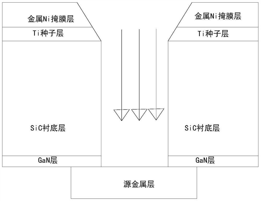
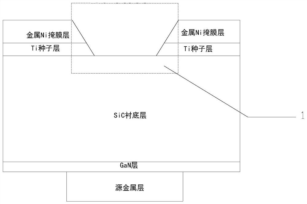
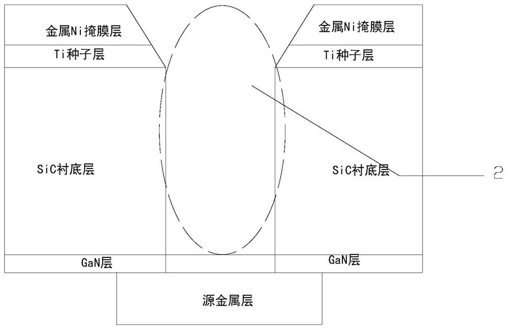
[0031] See Figure 1 to Figure 6 , a deep hole etching method for SiC-based GaN crystals, SiC-based GaN crystals (see figure 1 ) from bottom to top are the SiC substrate layer, GaN layer, and source metal layer. The deep hole etching is to perform dry etching on the SiC substrate layer and the GaN layer to form the back hole of the SiC-based GaN crystal. The complete etching steps (see Figure 5 )as follows:

[0032] S1: Pre-etching treatment, mechanically grind the SiC substrate layer to thin it to 90um-110μm, and then photolithography and deposit Ti on the back of the SiC substrate layer, thereby formi...


PUM

PropertyMeasurementUnit
thicknessaaaaaaaaaa
thicknessaaaaaaaaaa
depthaaaaaaaaaa

Abstract

The invention discloses a deep hole etching method of a SiC-based GaN crystal. The deep hole etching method mainly comprises the steps of processing before etching, etching a pre-etched hole, performing first dry etching on a SiC substrate layer under a first etching parameter, performing second dry etching on a GaN base layer under a second etching parameter, and finally forming a back hole by etching. When the etching method is used for etching the SiC-based GaN crystal with a large size, particularly six inches, the selective ratio of SiC to GaN is larger than 30:1 during etching of the SiC substrate, the selective ratio of the SiC to Ni is larger than 30:1, the side wall angle is 85-87 degrees, the selective ratio of the GaN to the SiC is larger than 3:1 during etching of the GaN base layer, the side wall angle is larger than 85 degrees, the finally-etched back hole is low in particle pollution, weak in metal corrosion and uniform in hole etching, and the warpage of the device can be effectively controlled.

Description

technical field [0001] The invention relates to the fields of field effect transistor (FET) and compound semiconductor technology, in particular to a SiC backhole etching method for SiC-based GaN crystals. Background technique [0002] As the third-generation wide bandgap compound semiconductor device, AlGaN / GaN HEMT has excellent characteristics in terms of power output and frequency characteristics, making it have a good application prospect in high temperature, high frequency, and high power devices. At present, SiC is selected as the preferred substrate material of AlGaN / GaN HEMT to manufacture SiC-based AlGaN / GaN HEMT devices. [0003] For SiC-based AlGaN / GaN HEMT devices, through-hole grounding is required to improve the frequency characteristics and reliability of the device, and facilitate the design and manufacture of microwave monolithic integrated circuits. At present, the through-holes of SiC-based AlGaN / GaN HEMT devices are selected for SiC Dry etching based on...

Claims


Application Information

Patent Timeline
Patent Type & Authority Patents(China)
IPC IPC(8): H01L21/3213H01L21/335H01L29/778
CPCH01L21/32136H01L29/66446H01L29/778
Inventor 王珺楠
Owner CHENGDU HIWAFER SEMICON CO LTD
Why Eureka
Try Eureka