Fabrication method of nanowire structure

A production method and nanowire technology, which are applied in nanotechnology, semiconductor devices, electrical components, etc., to achieve the effect of small damage

Active Publication Date: 2020-02-11
INST OF MICROELECTRONICS CHINESE ACAD OF SCI +1
View PDF5 Cites 0 Cited by
  • Summary
  • Abstract
  • Description
  • Claims
  • Application Information

AI Technical Summary

Problems solved by technology

[0007] The main purpose of this application is to provide a method for manufacturing a nanowire structure, so as to solve the problem that the manufacturing method in the prior art cannot control the etching of the first semiconductor well under the premise of ensuring less damage to other material layers The problem of the speed of the material department

Method used


Image

  • Fabrication method of nanowire structure
  • Fabrication method of nanowire structure
  • Fabrication method of nanowire structure

Examples


Embodiment 1

[0089] The nanowire fabrication process includes:

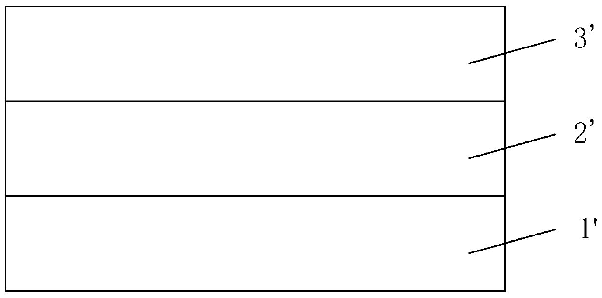
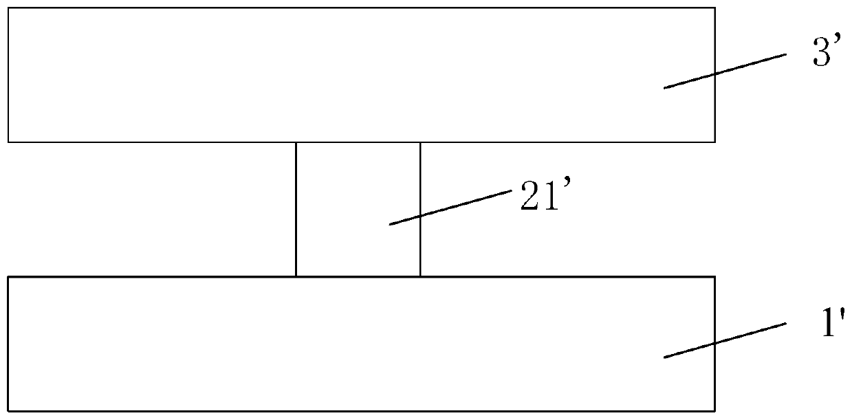
[0090] Step S1, providing a substrate, which is a silicon substrate, and sequentially epitaxially growing germanium and vapor-phase-depositing silicon nitride on the above-mentioned substrate, and then forming a first semiconductor material layer with a thickness of 40 nm and a mask with a thickness of 40 nm. The film layer is etched through the mask layer, the first semiconductor material layer and the silicon substrate at a certain depth by plasma anisotropic etching to form an island structure with steep side walls. The width of the island structure is 100nm. Each island structure includes The first semiconductor material part and the mask part.

[0091] Step S2, oxidizing the first semiconductor material part and the substrate in each island structure, so that the surface part of the first semiconductor material part forms the first surface layer 20, that is, the germanium oxide layer, and the surface part of the substrat...

Embodiment 2

[0097] The difference from Example 1 is that

[0098] In step S2, the gas pressure in the plasma oxidation device is controlled to be 5mT, the radio frequency power of the plasma oxidation device is controlled to be 100W, the temperature in the plasma oxidation device is controlled to be 100°C, and oxygen is introduced into the device, In addition, the flow rate of oxygen is 5 sccm, and the working time of the radio frequency source for controlling the plasma oxidation device is 10 s.

[0099] Step S3, using a dry etching device to etch and remove the above-mentioned first surface layer, that is, putting the structure processed in step S2 into a dry etching device, specifically, controlling the gas pressure in the above-mentioned etching device to be 5 mT, and controlling The radio frequency power of the above-mentioned etching device is 50W, the temperature in the device is controlled to be 100°C, the etching gas HCl and the carrier water vapor are passed into the device, and...

Embodiment 3

[0101] The difference from Example 1 is that

[0102] In step S2, the gas pressure in the plasma oxidation device is controlled to be 100mT, the radio frequency power of the plasma oxidation device is controlled to be 100W, the temperature in the plasma oxidation device is controlled to be 150°C, and oxygen is introduced into the device, And the flow rate of oxygen is 200 sccm, and the working time of the radio frequency source for controlling the plasma oxidation device is 2s.

[0103] In step S3, a dry etching device is used to etch and remove the above-mentioned first surface layer, that is, the structure processed in step S2 is put into a dry etching device, specifically, the gas pressure in the above-mentioned etching device is controlled to be 100 mT, Control the radio frequency power of the above-mentioned etching device to 100W, control the temperature in the device to 150°C, pass the etching gas HCl and carrier water vapor into the device, and the flow rate of HCl is ...


PUM

PropertyMeasurementUnit
thicknessaaaaaaaaaa

Abstract

The invention provides a method for manufacturing a nanowire structure. The method comprises the following steps: step S1, providing a substrate, and forming a first semiconductor material and a mask part, which are away from the substrate, on the substrate; step S2, performing surface treatment on the first semiconductor material, so that the surface part of the first semiconductor material forms a first surface layer; step S3, etching to remove the first surface layer, wherein the ratio of the removal rate of the first surface layer to the removal rate of the substrate is greater than 10; and repeating step S2 and step S3, until a first semiconductor material forms a nanowire. By adoption of the method, self-limiting etching is realized, and relatively small damage to the substrate in the etching process is guaranteed; and then the surface treatment is performed, and the etching is performed until the nanowire structure with a predetermined size is formed, and mover the repeatability and the uniformity of the formed nanowire structure are good.

Description

technical field [0001] The present application relates to the field of semiconductors, in particular, to a method for fabricating a nanowire structure. Background technique [0002] The nanowire structure is generally used as the structure of an advanced MOS device (such as a channel). In semiconductor manufacturing, the manufacturing process of the nanowire generally includes: growing the first semiconductor material part 2' and the second semiconductor material part 2' sequentially on the substrate 1' by epitaxy. material section 3', formed as figure 1 The structure shown; a part of the first semiconductor material part 2' is selectively removed, and the remaining first semiconductor material part forms a nanowire 21', such as figure 2 shown. [0003] In the prior art, wet etching, plasma dry etching or gaseous molecular reaction etching is generally used to remove the first semiconductor material part. Hereinafter, the substrate is a silicon layer, the first semiconduc...

Claims


Application Information

Patent Timeline
Patent Type & Authority Patents(China)
IPC IPC(8): H01L29/06B82Y40/00
CPCB82Y40/00H01L29/0676
Inventor 李俊杰崔虎山朱慧珑赵超
Owner INST OF MICROELECTRONICS CHINESE ACAD OF SCI
Why Eureka
Try Eureka