Non-junction tunneling field effect transistor and manufacturing method thereof

A tunneling field effect and transistor technology, applied in the field of electronics, can solve problems such as structure and preparation method to be improved, complex process, impurity diffusion, etc., and achieve the effects of avoiding trap-assisted tunneling, simple process, and increasing gate oxide thickness

Active Publication Date: 2017-11-10
TSINGHUA UNIV
View PDF4 Cites 3 Cited by
  • Summary
  • Abstract
  • Description
  • Claims
  • Application Information

AI Technical Summary

Problems solved by technology

However, the traditional tunneling transistor needs to use ion implantation and high temperature annealing process to form the tunneling junction. The heat dissipation is large, the process is complicated, and there is impurity diffusion, so it is difficult to form a small-sized abrupt junction.
The junctionless field effect transistor does not require ion implantation to form a junction, but it still relies on the drift and diffusion of carriers to work, so the subthreshold swing is also limited by 60mV / dec
[0003] Therefore, whether it is the current junctionless field effect transistor or the tunneling field effect transistor, its structure and preparation method still need to be improved.

Method used


Image

  • Non-junction tunneling field effect transistor and manufacturing method thereof
  • Non-junction tunneling field effect transistor and manufacturing method thereof
  • Non-junction tunneling field effect transistor and manufacturing method thereof

Examples


Embodiment Construction

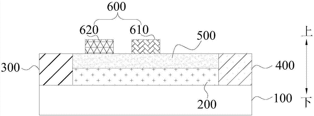
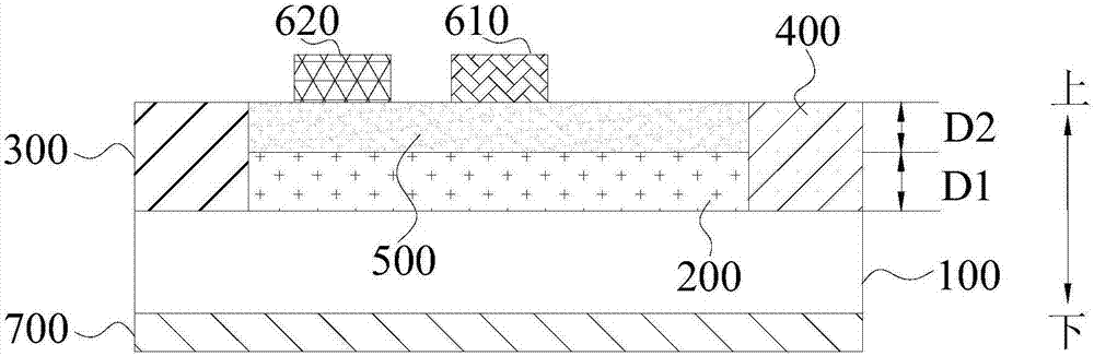
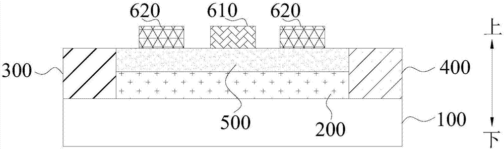
[0030] Embodiments of the present invention are described in detail below, examples of which are shown in the drawings, wherein the same or similar reference numerals designate the same or similar elements or elements having the same or similar functions throughout. The embodiments described below by referring to the figures are exemplary only for explaining the present invention and should not be construed as limiting the present invention.

[0031] In the description of the present invention, the orientations or positional relationships indicated by the terms "upper", "lower" and the like are based on the orientations or positional relationships shown in the accompanying drawings, which are only for the convenience of describing the present invention and do not require that the present invention must be based on a specific Azimuth configuration and operation, therefore, should not be construed as limiting the invention.

[0032] The fact that a first feature is "on" or "unde...


PUM


Abstract

The invention provides a non-junction tunneling field effect transistor and a manufacturing method thereof. The non-junction tunneling field effect transistor comprises an insulation layer, a channel region arranged on the insulation layer, and a source electrode and a drain electrode which are arranged at two sides of the channel region, a gate medium layer arranged on the channel region, and a grid electrode which is arranged on the gate medium layer and comprises a top grid and a static modulation grid electrode. The non-junction tunneling field effect transistor has at least one of advantages as follows, simple structure, easy realization through utilizing the relatively simple process, flexible and adjustable doping concentration and relatively low power consumption.

Description

technical field [0001] The invention relates to the field of electronics, in particular to a junctionless tunneling field effect transistor and a preparation method. Background technique [0002] The subthreshold swing of tunneling field effect transistors can reach a value lower than 60mV / dec at room temperature, breaking through the limit of traditional field effect transistors. This makes it have a good application prospect in the field of low-power integrated circuits in the future. However, the traditional tunneling transistor needs to use ion implantation and high-temperature annealing process to form the tunneling junction. The heat dissipation is large, the process is complicated, and there is impurity diffusion, so it is difficult to form a small-sized abrupt junction. The junctionless field effect transistor does not require ion implantation to form a junction, but it still relies on the drift and diffusion of carriers to work, so the subthreshold swing is also li...

Claims


Application Information

Patent Timeline
Patent Type & Authority Applications(China)
IPC IPC(8): H01L29/739H01L21/331
CPCH01L29/66356H01L29/7391
Inventor 张书琴梁仁荣王敬许军
Owner TSINGHUA UNIV
Why Eureka
Try Eureka