Quantum dot electroluminescence device and manufacturing method thereof

一种电致发光器件、量子点发光的技术,应用在电固体器件、半导体/固态器件制造、电气元件等方向,能够解决降低器件发光效率、电子与空穴不平衡、降低材料发光效率等问题,达到提升器件发光效率、减小能垒的效果

Inactive Publication Date: 2017-11-10
TCL CHINA STAR OPTOELECTRONICS TECH CO LTD
View PDF6 Cites 19 Cited by
  • Summary
  • Abstract
  • Description
  • Claims
  • Application Information

AI Technical Summary

Problems solved by technology

[0003] At present, there is a big gap between the luminous efficiency of QLED and OLED. On the one hand, because the material of the QD (quantum dot) light-emitting layer in QLED is prepared by a solution method, the material itself has many defect states, thereby reducing the luminous efficiency of the material; On the one hand, in terms of device structure design, in order to obtain high-efficiency devices, it is necessary to balance the carrier concentration injected into the light-emitting layer. In OLED design, since the energy level of the light-emitting layer material is moderate, a variety of functional layer materials can be selected to match its energy level. (Energy barrier1eV), and electron injection has almost no energy barrier, resulting in a serious imbalance between electrons and holes, thereby reducing the luminous efficiency of the device

Method used


Image

  • Quantum dot electroluminescence device and manufacturing method thereof
  • Quantum dot electroluminescence device and manufacturing method thereof
  • Quantum dot electroluminescence device and manufacturing method thereof

Examples


Embodiment Construction

[0017] Hereinafter, embodiments of the present invention will be described in detail with reference to the accompanying drawings. This invention may, however, be embodied in many different forms and should not be construed as limited to the specific embodiments set forth herein. Rather, the embodiments are provided to explain the principles of the invention and its practical application, thereby enabling others skilled in the art to understand the invention for various embodiments and with various modifications as are suited to particular intended uses.

[0018] In the drawings, the shapes and dimensions of elements may be exaggerated for clarity, and the same reference numerals will be used throughout to designate the same or like elements.

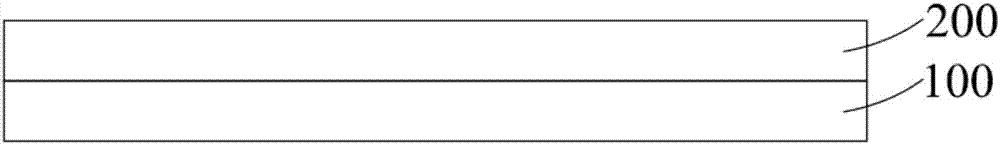
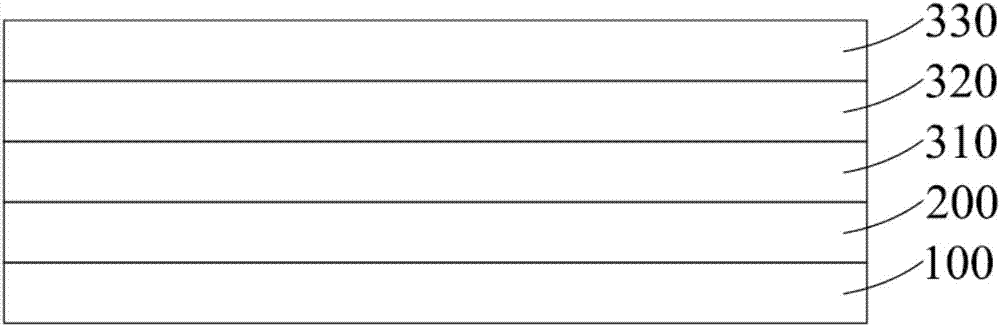
[0019] Figure 1A to Figure 1F It is a process chart of the manufacturing method of the quantum dot electroluminescent device according to the first embodiment of the present invention.

[0020] The fabrication method of the quantum dot...


PUM


Abstract

The invention provides a quantum dot electroluminescence device. The quantum dot electroluminescence device comprises a substrate, an anode, hole transport layers, a quantum dot luminescence layer, an electron transport layer and a cathode, wherein the anode is arranged on the substrate; the hole transport layers are arranged on the anode; the quantum dot luminescence layer is arranged on the hole transport layers; the electron transport layer is arranged on the quantum dot electroluminescence layer; the cathode is arranged on the electron transport layer; and the hole transport layers are P-type doped hole transport layers and / or the electron transport layer is an N-type doped electron transport layer. The invention also provides a manufacturing method of the quantum dot electroluminescence device. A gradient doping effect is formed in the hole transport layers, different band bending degrees of an interface are caused, a ladder energy level is formed, namely HOMO energy level is gradually increased from the anode to the quantum dot luminescence layer in sequence, and then the energy barrier of holes from the injection of the anode to the quantum dot luminescence layer is reduced, so that the luminescence efficiency of the device is improved.

Description

technical field [0001] The invention belongs to the technical field of electroluminescence, and in particular relates to a quantum dot electroluminescence device and a manufacturing method thereof. Background technique [0002] Quantum dot electroluminescent devices (QLEDs) can actively emit light like OLEDs, and have the advantages of fast response, wide viewing angles, thinness, and low power consumption. At the same time, compared with OLEDs, they have higher color purity and can be used in display devices. Wide color gamut. Quantum dot materials can be easily dissolved in a variety of solvents by changing the surface ligands, which is very suitable for low-cost solution processing. [0003] At present, there is a big gap between the luminous efficiency of QLED and OLED. On the one hand, because the material of the QD (quantum dot) light-emitting layer in QLED is prepared by a solution method, the material itself has many defect states, thereby reducing the luminous effi...

Claims


Application Information

Patent Timeline
Patent Type & Authority Applications(China)
IPC IPC(8): H01L51/50H01L51/56
CPCH10K50/11H10K2101/40H10K50/115H10K50/156H10K50/166H10K71/00H10K71/30H10K50/155H10K50/165H10K2101/80
Inventor 周凯锋
Owner TCL CHINA STAR OPTOELECTRONICS TECH CO LTD
Why Eureka
Try Eureka