
APD bias control circuit, photoelectric receiving circuit and bias control method

A bias control and circuit technology, applied in the optical field, can solve the problems of large wiring space occupied by circuit components, increase in the number of circuit components, and increase the total power consumption of photoelectric receiving circuits, etc., to meet the requirements of circuit miniaturization and low power consumption , The effect of less circuit components

Active Publication Date: 2020-08-25
INNOLIGHT TECHNOLOGY (SUZHOU) LTD
View PDF7 Cites 0 Cited by
  • Summary
  • Abstract
  • Description
  • Claims
  • Application Information

AI Technical Summary

Problems solved by technology

[0004] The inventor found in the process of realizing the present invention that a multi-channel high-speed photoelectric receiving circuit based on multiple APDs has been proposed at present, such as the multi-channel optical transmission link of IEEE 100G ER4 40km disclosed in IEEE802.3ba-2010; The APD bias control circuit can not provide bias voltage and overload protection for multiple APDs at the same time. Therefore, when it is necessary to provide bias voltage and overload protection for multiple APDs in the multi-channel photoelectric receiving circuit The characteristic parameters of each APD (such as the reverse breakdown voltage Vbr) configure a set of APD bias control circuits for each APD, which will not only increase the total power consumption of the photoelectric receiving circuit to a large extent, but also due to Due to factors such as the increase in the number of circuit components required by the photoelectric receiving circuit and the large wiring space occupied by the circuit components, the photoelectric receiving circuit cannot meet the requirements of circuit miniaturization.

Method used


Image

  • APD bias control circuit, photoelectric receiving circuit and bias control method
  • APD bias control circuit, photoelectric receiving circuit and bias control method
  • APD bias control circuit, photoelectric receiving circuit and bias control method

Examples


Embodiment 1

[0025] Embodiment 1, APD bias voltage control circuit.

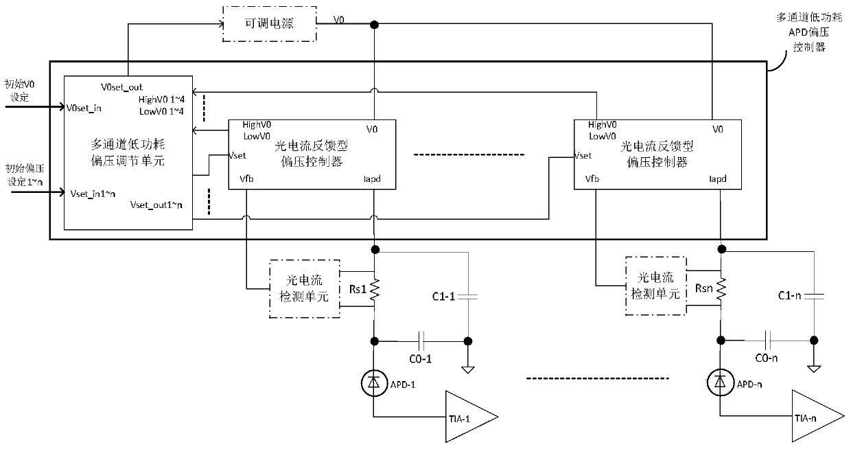
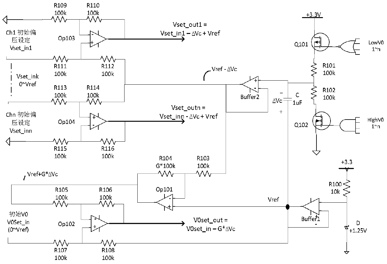
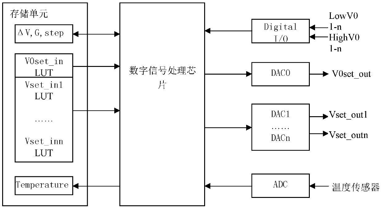
[0026] The APD bias voltage control circuit of this embodiment is mainly suitable for multi-channel photoelectric receiving circuits, that is, the APD bias voltage control circuit of this embodiment can provide stable load voltages for each APD in the multi-channel photoelectric receiving circuit at the same time (that is, load on the APD on the voltage). The main structure of the APD bias control circuit of this embodiment and the operations performed by each element are as follows Figure 1-7 shown.

[0027] The APD bias voltage control circuit will be described below with reference to specific embodiments.

[0028] figure 1 Among them, the APD bias voltage control circuit of this embodiment mainly includes: a bias voltage adjustment unit (ie figure 1 The multi-channel low-power bias adjustment unit in the) and n bias controllers (ie figure 1 In the photocurrent feedback bias controller), where n is an integer gre...

Embodiment 2

[0095] Embodiment 2, photoelectric receiving circuit.

[0096] The photoelectric receiving circuit in this embodiment mainly includes: a plurality of APDs, a plurality of photocurrent detection units (the number of photocurrent detection units is the same as the number of APDs), an APD bias control circuit and a power module; wherein, each APD Each APD is connected to a corresponding photocurrent detection unit, each APD is also connected to an APD bias voltage control circuit, each photocurrent detection unit is connected to a bias voltage control circuit, and the power module is connected to an APD bias voltage control circuit.

[0097] The photocurrent detection unit is mainly used to detect the photocurrent intensity voltage signal corresponding to the photocurrent signal of the APD connected to it.

[0098] The APD bias control circuit is mainly used to generate the power supply voltage control signal and the bias control signal of each APD according to the overvoltage st...

Embodiment 3

[0100] Embodiment 3, APD bias voltage control method.

[0101] The APD bias control method in this embodiment mainly includes the following steps:

[0102] Firstly, each bias controller generates overvoltage state indication information or undervoltage state indication information according to the photocurrent intensity voltage signal corresponding to the photocurrent signal flowing through the APD connected to it.

[0103] Specifically, each bias controller in this embodiment can be called a photocurrent feedback bias controller, and each bias controller mainly includes a bias voltage generation unit and a voltage follower unit, wherein the bias voltage The generating unit can generate overvoltage state indication information or undervoltage state indication information according to the photocurrent intensity voltage signal transmitted by the photocurrent detection unit.

[0104] Secondly, the bias voltage adjustment unit generates the power supply voltage control signal and...


PUM


Abstract

The invention provides an APD bias control circuit, a photoelectric receiving circuit and a bias control method. The APD bias control circuit comprises a bias regulation unit and a plurality of bias controllers, wherein the bias regulation unit is used for generating a supply voltage control signal and a bias control signal of each APD according to overvoltage state indication information and undervoltage state indication information transmitted by each bias controller; the plurality of bias controllers are connected with the plurality of APDs, used for receiving light current strength voltage signals corresponding to light current signals passing through the APDs connected with the bias controllers, and generating load voltage of the APDs connected with the bias controllers according to current supply voltage, the light current strength voltage signal and the bias control signal of a power module. According to the technical scheme of the circuits and method provided by the invention, the characteristics of few circuit element, low overall circuit power consumption and small wiring space occupied by circuit elements are achieved, and the requirement of miniaturization of the circuits is met, while multi-channel low power consumption APD bias control is achieved.

Description

technical field [0001] The invention relates to the field of optical technology, in particular to an APD bias voltage control circuit, a photoelectric receiving circuit and an APD bias voltage control method. Background technique [0002] APD (Avalanche Photo Diode, avalanche photodiode) has been widely used in light detection and other technologies due to its high sensitivity, fast response speed and wide frequency bandwidth. [0003] During the working process of the APD, it is usually necessary to use the APD bias voltage control circuit to control the reverse bias voltage applied to the APD, so that when the APD receives light, the APD will generate electrons under the action of the reverse bias voltage. The electron-hole pair will be collected by an external electric field and converted into a current, and the intensity of the converted current is usually proportional to the intensity of the light. In addition, the APD bias control circuit can also provide overload pro...

Claims


Application Information

Patent Timeline
Patent Type & Authority Patents(China)
IPC IPC(8): H03F3/08H04B10/69
CPCH03F3/082H04B10/6911
Inventor 王祥忠
Owner INNOLIGHT TECHNOLOGY (SUZHOU) LTD
Learn More