High-emission-rate and high-collection-efficiency single photon source device

A single-photon source, emission rate technology, applied in the field of quantum information and ion-polar photonics, to achieve the effect of improving emission rate and huge application value

Pending Publication Date: 2017-11-17
INST OF ELECTRONICS ENG CHINA ACAD OF ENG PHYSICS
View PDF4 Cites 14 Cited by
  • Summary
  • Abstract
  • Description
  • Claims
  • Application Information

AI Technical Summary

Problems solved by technology

However, the Purcell enhancement factor of photonic crystals and dielectric microcavities increased by single phot

Method used


Image

  • High-emission-rate and high-collection-efficiency single photon source device
  • High-emission-rate and high-collection-efficiency single photon source device
  • High-emission-rate and high-collection-efficiency single photon source device

Examples


Embodiment 1

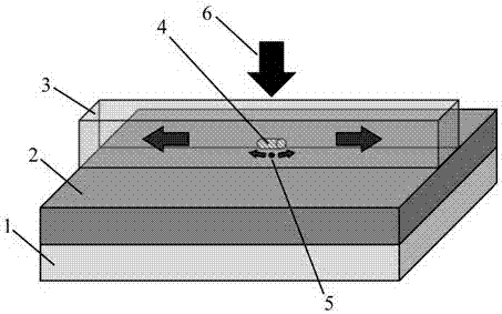
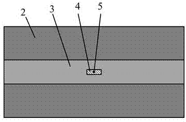
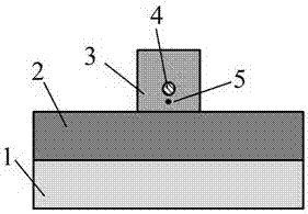
[0029] as attached figure 1 , 2 , 3, the present invention provides a single-photon source device with high emission rate and high collection efficiency based on gap plasmons and dielectric-carried surface plasmon waveguides, the single-photon source device includes SiO 2 A substrate 1 , a medium-carrying surface plasmon waveguide, a gap plasmon microcavity, and a quantum dot 5 .

[0030] The gap plasmon microcavity is composed of a metal thin film 2 and a metal nanorod 4 for forming a gap plasmon; wherein: the metal thin film 2 is a gold thin film, and the metal nanorod 4 is a gold nanorod.

[0031] The quantum dot 5 is located in the gap plasmon microcavity composed of the gold film 2 and the gold nanorod 4; the medium-loaded surface plasmon waveguide includes the gold film 2 and SiO 2 The dielectric strip 3 is used to collect photons emitted by the quantum dots 5 . The distance between the gold nanorod 4 and the gold film 2 is 10nm, the quantum dot 5 is located in the mi...

Embodiment 2

[0044] A high emission rate, high collection efficiency single-photon source device based on gap plasmons and dielectric-supported surface plasmon waveguides, such as figure 1 , 2 , 3, the single photon source device includes Si substrate 1, silver film 2, Si 3 N 4 Dielectric strip 3, gold nanorod 4 and fluorescent molecule 5.

[0045] The silver thin film 2 and the gold nanorod 4 constitute a gap plasmon microcavity, which is used to form a gap plasmon; the fluorescent molecule 5 is located in the gap plasmon microcavity composed of the silver thin film 2 and the gold nanorod 4; the silver Film 2 and Si 3 N 4 The dielectric strip 3 forms a dielectric-carried surface plasmon waveguide for collecting photons emitted by the fluorescent molecules 5 .

[0046]The distance between the gold nanorod 4 and the silver film 2 is 10nm, the fluorescent molecule 5 is located in the middle of the interstitial plasmon microcavity, and the distance from the upper surface of the silver fi...


PUM

PropertyMeasurementUnit
Thicknessaaaaaaaaaa
Diameteraaaaaaaaaa
Lengthaaaaaaaaaa

Abstract

The invention discloses a high-emission-rate and high-collection-efficiency single photon source device including a substrate, a metal film, a dielectric strip, a metal nanorod and a single photon source, the metal film is deposited on the substrate and the dielectric strip is deposited on the metal film, the metal film and the dielectric strip form the media-carrying surface plasmon waveguide, the media-carrying surface plasmon waveguide is used for collecting the photons emitted by the single photon source, the metal nanorod is arranged inside the media-carrying surface plasmon waveguide, the single photon source is arranged between the metal nanorod and the metal film, the metal film and the metal nanorod form a gap plasmon micro-cavity structure, the gap plasmon micro-cavity structure forms the gap plasmon to enhance the emission rate of the single photon source. The high-emission-rate and high-collection-efficiency single photon source device is advantageous in greatly enhancing the emission rate of the single photon source, improving the collection efficiency of the single photons, and achieving the oriented excitation of mode in the waveguide. The single photon source device has huge application values in the fields of quantum information and integrated photon devices.

Description

technical field [0001] The invention relates to the fields of single photon source technology, plasmon photonics and quantum information, and specifically refers to a single photon source device with high emission rate and high collection efficiency. Background technique [0002] A single photon source refers to a light source that emits only one photon at a time. It plays an important role in the field of quantum information, such as quantum key distribution, linear optical quantum computing, quantum secure communication, and quantum information processing. In addition, single photon sources also have important application value in the fields of precision measurement and bioluminescence labeling imaging. Materials commonly used to generate single photons include semiconductor quantum dots, fluorescent molecules, and diamond NV centers. Generally, the spontaneous emission rate of single-photon sources in free space is low, and the emission of single-photons is not direction...

Claims


Application Information

Patent Timeline
IPC IPC(8): H01L33/04
CPCH01L33/04
Inventor 黄锋李沫陈飞良张晖李倩张健
Owner INST OF ELECTRONICS ENG CHINA ACAD OF ENG PHYSICS
Why Eureka
Try Eureka