Preparation method of low-on-resistance high-threshold-value voltage enhancement type GaN device

A technology with high threshold voltage and low on-resistance, applied in semiconductor/solid-state device manufacturing, semiconductor devices, electrical components, etc., can solve the problem of low barrier layer, large square resistance in the p-GaN cap layer area, affecting device conduction characteristics, etc., to achieve the effect of high optimization space, low on-resistance, and reduction of mutual constraints

Inactive Publication Date: 2017-11-24
NO 55 INST CHINA ELECTRONIC SCI & TECHNOLOGYGROUP CO LTD
View PDF4 Cites 9 Cited by
  • Summary
  • Abstract
  • Description
  • Claims
  • Application Information

AI Technical Summary

Problems solved by technology

The current p-GaN cap layer threshold voltage modulation technology, because the material is grown at one time, the thickness of the barrier layer under the p-GaN cap layer is very thin, generally below 15nm, an

Method used


Image

  • Preparation method of low-on-resistance high-threshold-value voltage enhancement type GaN device
  • Preparation method of low-on-resistance high-threshold-value voltage enhancement type GaN device
  • Preparation method of low-on-resistance high-threshold-value voltage enhancement type GaN device

Examples


Embodiment Construction

[0022] The technical solutions of the present invention will be further described below in conjunction with the accompanying drawings and embodiments.

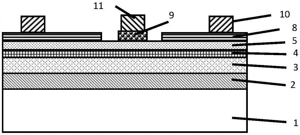
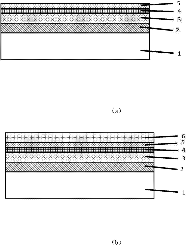
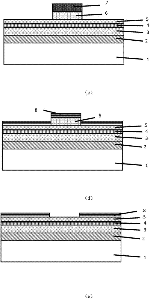
[0023] Such as figure 1 Shown is a schematic diagram of the GaN enhanced device structure with low on-resistance and high threshold voltage according to the present invention, and its preparation method includes growing a full-structure material growth with a buffer layer, a channel layer, an insertion layer, and a barrier layer; the outer channel Preparation of selective growth mask; definition of gate area mask; selective regrowth of outer channel layer structure and removal of mask; preparation of gate area selective growth mask; definition of gate regrowth area; gate area barrier layer re-growth Growth and removal of masks; preparation of ohmic contacts; preparation of gate contacts. Specifically include the following steps:

[0024] (1) On the substrate 1, utilize the epitaxial growth method to epitaxially grow the buff...


PUM

PropertyMeasurementUnit
Thicknessaaaaaaaaaa

Abstract

The invention discloses a preparation method of a low-on-resistance high-threshold-value voltage enhancement type GaN device. The preparation method specifically comprises the steps of performing epitaxial growth of a buffer layer, a channel layer, an inserting layer and a barrier layer on a substrate in sequence; preparing a selective growth mask layer; performing etching on an external channel selective growth mask layer; performing selective epitaxial growth of an external channel layer; removing a selective growth mask; preparing a selective growth mask layer; performing etching of a gate selective growth region mask layer; performing selective growth of the barrier layer; removing the selective growth mask layer and the external channel layer thereon; preparing source and drain metals and alloy; and preparing a gate metal. The enhancement type GaN device has the advantages of low on-resistance, high threshold value voltage and uniformity, high freedom degree of internal and external channel materials, no dynamic characteristic degradation problem of the device caused by loss and defects, and the like.

Description

technical field [0001] The invention belongs to the technical field of semiconductor device preparation, and in particular relates to a preparation method of a low on-resistance high threshold voltage enhanced GaN device. Background technique [0002] GaN wide bandgap semiconductor material has excellent characteristics and has significant advantages in the development of high-performance power devices. In particular, the characteristics of high critical breakdown field strength and high electron saturation drift rate of GaN material make it have important application prospects in the development of high operating frequency and high power switching devices. [0003] For power switching devices, in order to ensure the safety of the power system, the device needs to be in a normally closed state when it is not working. The GaN power switching device implemented by the commonly used AlGaN / GaN heterojunction structure is in the normally-on state. [0004] At present, the metho...

Claims


Application Information

Patent Timeline
IPC IPC(8): H01L29/778H01L21/335
Inventor 周建军孔岑郁鑫鑫张凯孔月婵
Owner NO 55 INST CHINA ELECTRONIC SCI & TECHNOLOGYGROUP CO LTD
Why Eureka
Try Eureka