Method for improving cut-off wavelength of indium arsenide/gallium antimony superlattice infrared detector material, indium arsenide/gallium antimony type II superlattice and application thereof

An infrared detector and cut-off wavelength technology, which is applied in semiconductor devices, photovoltaic power generation, electrical components, etc., can solve the problems of high growth cost, many intra-crystal interfaces, and low service life of production equipment, and achieve the effect of improving the detection wavelength

Active Publication Date: 2017-11-24
秦皇岛博硕光电设备股份有限公司
View PDF5 Cites 3 Cited by
  • Summary
  • Abstract
  • Description
  • Claims
  • Application Information

AI Technical Summary

Problems solved by technology

[0004] The purpose of the present invention is to provide a method for improving the difficulty of material growth, high material growth cost, and low service life of production equipment due to the many intracrystalline interfaces of indium arsenide / gallium antimony II superlattice in the prior art. Indium Arsenic / Gallium Antimony Superlattice Infrared Detector Material Cutoff Wavelength Method and Indium Arsenic / Gallium Antimony Type II Superlattice Material and Its Application

Method used


Image

  • Method for improving cut-off wavelength of indium arsenide/gallium antimony superlattice infrared detector material, indium arsenide/gallium antimony type II superlattice and application thereof
  • Method for improving cut-off wavelength of indium arsenide/gallium antimony superlattice infrared detector material, indium arsenide/gallium antimony type II superlattice and application thereof
  • Method for improving cut-off wavelength of indium arsenide/gallium antimony superlattice infrared detector material, indium arsenide/gallium antimony type II superlattice and application thereof

Examples


Embodiment Construction

[0024] Below in conjunction with specific embodiment and accompanying drawing, the present invention will be further described:

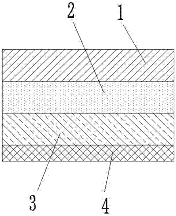
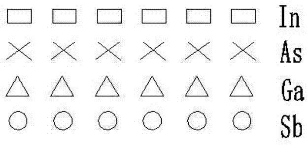
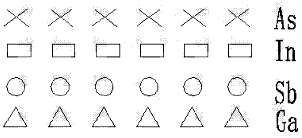
[0025] For the type II superlattice composed of InAs / GaSb, it has two basic material components, InAs and GaSb, for the type II superlattice material composed of InAs and GaSb, the arrangement of its elements has certain rules property, that is, the elements of Group V and Group III are arranged alternately in sequence, that is, one layer of Group V elements, one layer of Group III elements, one layer of Group V elements, and one layer of Group III elements are arranged in sequence, or one layer of Group III elements, one layer of Group III elements The elements of group v, one layer of group III elements and one layer of group v elements are arranged alternately in sequence. With different element arrangements, the InAs layer and the GaSb layer in the InAs / GaSb II superlattice form different interfacial layers in the unit cell, such as figure 2 A...


PUM


Abstract

The invention aims to provide a method for improving a cut-off wavelength of an indium arsenide / gallium antimony superlattice infrared detector material, an indium arsenide / gallium antimony type II superlattice material and an application thereof aiming at the defects that the growth difficulty of the material is increased, the growth cost of the material is high, and the service life of production equipment is short due to excessive intracrystalline interfaces of indium arsenide / gallium antimony type II superlattices in the prior art. According to the method for improving the cut-off wavelength of the indium arsenide / gallium antimony superlattice infrared detector material, the cut-off wavelength of the indium arsenide / gallium antimony type II superlattice infrared detector material can be increased by increasing the stress of an InSb layer in an indium arsenide / gallium antimony type II superlattice unit cell and changing the energy band structure of the superlattice material. By adopting the method provided by the invention, the cut-off wavelength of the superlattice infrared detector material can be increased by changing the energy band structure, obtained devices prepared from the indium arsenide / gallium antimony type II superlattice material has higher detectivity, the number of material interfaces can be reduced, the levels can be reduced, and the detection wavelength and detectivity of the indium arsenide / gallium antimony type II superlattice material can be further increased.

Description

technical field [0001] The invention relates to the technical field of indium arsenic / gallium antimony type II superlattice and infrared detector materials, in particular to indium arsenic / gallium antimony type II superlattice materials and improving the cutoff wavelength of indium arsenic / gallium antimony superlattice infrared detector materials method. The present invention improves the lattice layer structure of the second type of superlattice composed of InAs / GaSb and provides a method for increasing the cut-off wavelength of the second type of superlattice material and discloses the indium arsenic of the structure of the present invention / Gallium antimony II superlattice material application. Background technique [0002] Compared with other infrared detectors, InAs / GaSb II superlattice infrared detectors have precise and controllable response bands, wide response bands, high operating temperature, long carrier lifetime, high quantum efficiency, low dark current and ...

Claims


Application Information

Patent Timeline
Patent Type & Authority Applications(China)
IPC IPC(8): H01L31/0304H01L31/0352H01L31/0368H01L31/111
CPCH01L31/0304H01L31/035236H01L31/0368H01L31/111Y02E10/50Y02P70/50
Inventor 曹耀辉陈建桥
Owner 秦皇岛博硕光电设备股份有限公司
Why Eureka
Try Eureka