Device and method for the continuous treatment of solids by means of a laser beam

A laser beam, solid-state technology, applied in laser welding equipment, welding equipment, metal processing equipment, etc., can solve problems such as high cost and material loss, and achieve the effect of reducing manufacturing costs

Active Publication Date: 2020-11-20
SILTECTRA
View PDF7 Cites 0 Cited by
  • Summary
  • Abstract
  • Description
  • Claims
  • Application Information

AI Technical Summary

Problems solved by technology

However, chipping processing is disadvantageous, for example, when solid materials are expensive or expensive to produce, such as semiconductor materials or sapphire or silicon carbide, because chipping, for example, causes significant material losses and thus high costs in the case of very thin wafers.
Furthermore, in the case of very thin wafers with large diameters, considerable thickness differences can be determined due to the ablation process, whereby the wafers can only be used for certain applications

Method used


Image

  • Device and method for the continuous treatment of solids by means of a laser beam
  • Device and method for the continuous treatment of solids by means of a laser beam
  • Device and method for the continuous treatment of solids by means of a laser beam

Examples


Embodiment Construction

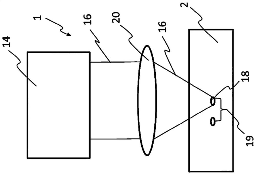
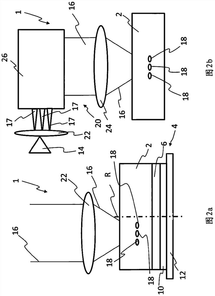
[0044] Figure 1a A laser device 14, a solid body 2 irradiated with a laser beam 16 of the laser device 14 and an optical device 20 arranged between the laser device 14 and the solid body 2 are schematically shown in a possible arrangement in the device 1 according to the invention. The optical device 20 is preferably arranged and designed in such a way that a modification 18, in particular a lattice change, such as a crack or a local phase transformation, can be formed on the surface of the solid 2 or in the interior of the solid 2, ie with the solid 2. The surfaces are generated spaced apart. The modification is particularly preferably produced in the focal point of the laser radiation. The laser device 14 here emits laser radiation 16 with a preferred pulse duration in the range of preferably 100 fs to 1 ps and particularly preferably in the range of 5 fs and 10 ps. An application of the laser beam in the aforementioned range is advantageous since only a small or no therma...


PUM


Abstract

The invention relates to a plant (1) for treating solids (2). The device according to the invention comprises: at least one containment device (4) having a containment part (6) for containing solids (2) and a holding part (10) for holding said containment part (6) , wherein the receiving part (6) can be driven continuously by means of a drive device; a laser device (14) for supplying a laser beam (16) to the solid body (8) or to the solid body A modification (18) is produced on the surface (20) of (2); and an optical device (20) for directing the laser beam (16), wherein the laser beam (16) can be Said optical device (20) is turned so that one or more solid bodies (2) can be irradiated by said laser beam (16) at different positions.

Description

technical field [0001] The invention according to claim 1 relates to an apparatus for processing solids and according to claim 15 to a method for processing solids. Background technique [0002] There are various types of solid processing such as ion implantation, etching, coating or ablation machining. However, chipping processing is disadvantageous, for example, when solid materials are expensive or expensive to produce, such as semiconductor materials or sapphire or silicon carbide, because chipping, for example, causes significant material losses and thus high costs in the case of very thin wafers. . Furthermore, in the case of very thin wafers with large diameters, considerable thickness differences can be determined due to the ablation process, so that the wafers can only be used for certain applications. Thickness fluctuations can be caused, for example, by vibrations of the sawing element. Contents of the invention [0003] It is therefore an object of the prese...

Claims


Application Information

Patent Timeline
Patent Type & Authority Patents(China)
IPC IPC(8): B23K26/00B23K26/0622B23K26/08B23K26/082B23K26/352B23K26/53
CPCB23K26/0624B23K26/082B23K26/352B23K26/359B23K26/53B23K26/0823B23K26/0006B23K2101/40B23K2103/50B23K2103/52B23K2103/56B29C59/002B29C59/16
Inventor 扬·黎克特马尔科·斯沃博达
Owner SILTECTRA
Why Eureka
Try Eureka